Optoelectronic Ceramic Packaging Solutions
Featured Product from Advanced Technical Ceramics Company
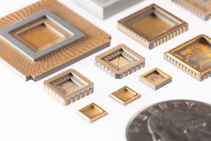
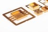
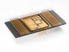
Advanced Multilayer Packaging for Optoelectronics Applications
- Multilayer AlN FPA substrates up to 110 mm x 110 mm[4.3” x 4.3”] in size with thin film metallization
- Flatness of less than 5 microns
- Nonmagnetic packaging options
- Multiple interfaces for connectors
- Hermiticity rates greater than 1 x 10^-8 cc He/s
- High temperature to cryogenic applications
- High power feedthroughs
- Military, Aerospace & Medical Applications
About AdTech Ceramics:
- 30+ years of ceramics Manufacturing
- 15+ years of Aluminum Nitride (AlN) Multilayer Technology
- Ceramic Injection molding
- Microwave Modeling & Design