NY Creates bets big on high NA EUV access
 
View web version 11 November 2026 — Issue 11 | Vol 18
 
Semiconductor Manufacturing — GlobalSpec
 

Source Products  |  Webinar Library  |  Standards

NY Creates bets big on high NA EUV access

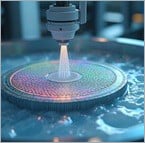
NY Creates bets big on high NA EUV access

The research hub also talks about the rise of regional ecosystems. Read more →

Take vacuum process control to the next level

Micro-Epsilon Group

Take vacuum process control to the next level

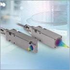
confocalDT high-temperature sensors deliver nanometer resolution, low outgassing and reliable wafer gap and layer thickness measurements up to 200° C, with UHV-compatible options for demanding vacuum processes.
 

View more
20 nm yield protection

Particle Measuring Systems

20 nm yield protection

At 20 nm, contamination drives yield, not just performance. Particles evade traditional monitoring, quietly damaging process integrity. Gain complete visibility and control across your water and chemical processes.
 

Learn more
On-demand: Specify dew point measurement for semiconductor dry gases

Vaisala

On-demand: Specify dew point measurement for semiconductor dry gases

Learn best practices for accurate dew point measurement in ultra-dry gases and wafer testing to reduce contamination risk, improve reliability, support sensor selection and support confident specification decisions.
 

View more
First high-volume 300 mm GaN to be established in Europe

First high-volume 300 mm GaN to be established in Europe

Infineon Technologies will invest about $1.23 billion in the project by 2034. Read more →

Applied Materials unveils its $5 billion EPIC Center

Applied Materials unveils its $5 billion EPIC Center

It is called the world’s largest facility dedicated to collaborative semiconductor process technology and manufacturing equipment R&D. Read more →

Design humidity control into semiconductor manufacturing environments

Vaisala

Design humidity control into semiconductor manufacturing environments

Explore where accurate humidity measurement supports contamination control, process stability, product quality and informed design decisions for semiconductor facilities, process areas and gas monitoring systems.
 

View more
Infineon shores up SiC supply security with Wolfspeed

Infineon shores up SiC supply security with Wolfspeed

An agreement will transform the existing relationship from 150 mm wafers to 200 mm substrate technology. Read more →

METIS HP: High-speed stability with high straightness motion system

ETEL S.A.

METIS HP: High-speed stability with high straightness motion system

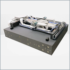
METIS HP delivers exceptional speed stability and dynamic straightness for high-end tools, handling panels up to 600 by 600 mm.
 

View more
CMP slurry selection for different wafer materials

Beijing Grish Hitech Co., Ltd.

CMP slurry selection for different wafer materials

Semiconductor industry CMP slurry guide matches wafer materials for higher removal rate and quality.
 

Learn more
Ceramic chucks for semiconductor wafer clamping and particle control

Fountyl Technologies Pte. Ltd.

Ceramic chucks for semiconductor wafer clamping and particle control

Alumina and silicon carbide chucks deliver ±1% vacuum uniformity, low particle risk and stable clamping in semiconductor manufacturing.
 

View more
   

GlobalSpec publishes more than 60 free industry newsletters - browse our portfolio.

Want to reach industry executives with your message? Download our media kit or contact us directly at sales@globalspec.com.

About this email: You are receiving this message as part of your complimentary newsletter subscription to Semiconductor Manufacturing. If you no longer wish to receive this newsletter, you can modify your preferences or unsubscribe.


Copyright © 2026 %%Member_Busname%%, Unless otherwise noted. All rights reserved.
%%Member_Busname%% | %%Member_Addr%% | %%Member_City%%, %%Member_State%% %%Member_PostalCode%%