CIQTEK Electron Microscope Versatile Detectors
Featured Product from CIQTEK Co., Ltd
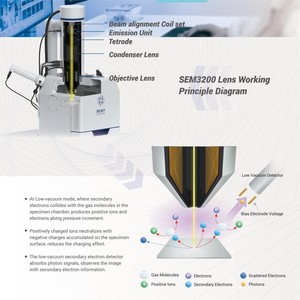
The scanning electron microscope (SEM) is used not only for the observation of surface morphology but also for the analysis of the composition of micro-regions on the specimen surface.
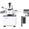
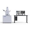
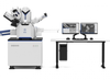
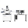
CIQTEK SEM3200 has a large specimen chamber with an extensive interface. In addition to supporting conventional Everhart–Thornley detector (ETD), Backscattered-Electron detector (BSE), and Energy-dispersive X-ray spectroscopy (EDS/EDX), various interfaces such as Electron Backscatter Diffraction Pattern (EBSD) and Cathodoluminescence (CL) are also reserved.
Backscattered-Electron Detector (BSE)
In the backscattered electron imaging mode, the charge effect is significantly suppressed and more information on the composition of the specimen surface can be observed.
Four-quadrants Backscattered Electron Detector - Multi-channel Imaging
The detector has a compact design and high sensitivity. With the 4-quadrants design, it is possible to obtain topographic images in different directions as well as composition distribution images without tilting the specimen.
Electron Backscatter Diffraction Pattern (EBSD)
The tungsten filament electron microscope with a large beam current fully meets the testing requirements of high-resolution EBSD and can analyze polycrystalline materials such as metals, ceramics, and minerals for crystal orientation and grain size analysis.
The figure shows the EBSD grain map of Ni metal specimen, which can identify grain size and orientation, determine grain boundaries and twins, and make accurate assessments of material organization and structure.