About

As market demand for smaller, faster and more capable devices creates challenges throughout the value chain, manufacturers are being forced to adapt and innovate. ESI's laser-based manufacturing solutions deliver that innovation by enabling customers to optimize their production capabilities and maintain high-volume manufacturing without sacrificing quality. Leveraging our laser-material interaction expertise, ESI can help you stay competitive and respond to new challenges by incorporating next-generation materials and new processes into your production flow.
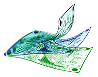
Laser Via Drilling Flex-PCB, HDI, Packaging
A via drilling portfolio that includes the most popular line of flex PCB processing systems, a CO2-laser-based system for affordable HDI PCB manufacturing and high-volume low cost-of-ownership solutions for IC packaging.
Wafer Processing Grooving, Dicing, Marking
Wafer processing and memory repair solutions that apply optimized laser technology to maintain high-volume production without sacrificing yield. Even when processing thin wafers or incorporating new materials.
Laser Ablation and Micro Machining
Cut, drill, weld and engrave on glass, leather, ceramic or metal. Or discover the composition of materials. Laser micromachining and laser ablation systems enable powerful laser processing.
Component Processing Resistor Trim, MLCC Test
A legacy of leadership that includes our CircuitTrim™ solutions for thick-film and thin-film resistor trimming, the industry standard for high-volume MLCC testing and the market-leading laser solution for production wafer trimming.
Supplier Directory Categories
Electro Scientific Industries, Inc. is listed in these categories: