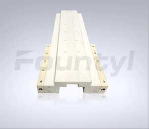
1600mm Ultra-Precision SiC Guide Rail
Featured Product from Fountyl Technologies Pte. Ltd.
In semiconductor photolithography systems, motion accuracy directly determines wafer exposure quality. Silicon carbide ceramic guide rails are critical structural components within ultra-precision motion platforms, enabling nanometer-level positioning under high-speed dynamic conditions.
With over 20 years of expertise in semiconductor ceramics, these ultra-precision SiC guides are engineered for advanced lithography and wafer handling systems.
Nanometer-Level Motion Performance
-
Designed for high-speed air-floating motion platforms
-
Supports ultra-precision wafer transport and alignment
-
Ensures stable trajectory control during exposure processes
Enables loading, alignment, measurement, and exposure with extreme positional accuracy.
Outstanding Material Properties
-
High flexural strength
-
Excellent corrosion and oxidation resistance
-
Superior wear resistance and low friction coefficient
-
High thermal conductivity
-
Excellent thermal shock resistance
Maintains dimensional stability in demanding cleanroom and high-temperature environments.
Optimized for Semiconductor Equipment
Applications include:
-
SiC air-floating motion platforms
-
Ultra-precision moving stages
-
Guide rails and slide rails
-
Vacuum suction components
-
Reflectors, crossbeams, and wafer tables
Supports high-speed, high-precision wafer motion in advanced lithography tools.
Engineering & Manufacturing Advantages
-
Japanese-based technology with independent R&D and production
-
Maximum length up to 1600 mm
-
Lightweight structural customization available
-
High-precision machining based on customer accuracy requirements
-
Optional materials: silicon carbide or alumina ceramic
By combining material stability, structural rigidity, and precision machining capability, these silicon carbide guide rails help semiconductor equipment manufacturers achieve higher throughput, tighter tolerances, and improved long-term system reliability.
Contact us to discuss your lithography platform requirements.


