Understanding HDI Flex Circuit Technology
Featured Product from PFC Flexible Circuits Limited

HDI Flex Circuit Technology
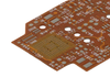
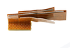
PFC’s high density capabilities offer customers a wide variety of custom flexible circuits with features such as extended lengths, multilayer, non- traditional material constructions, and specialized foils. The properties of flex-based materials enable smaller applications with the benefit of reduced weight and optimized packaging utilization. Our goal is to facilitate new designs that require smaller footprints and ultradense and precise conductor geometries.
PFC Recommended Design GuidelinesAdvances in materials and etching technologies have made HDI – high density flex geometries attainable. Standard copper clad-foil for HDI flex circuitry has 18-microns thick copper and, in some cases, thinner. Material choices are a large factor in PFC’s ability to provide cost-effective, high-density circuits.
- HDI flex circuit technology leader for over a decade.
- Experienced builders of production 50-micron trace and space.
- Provider of 37.5-micron trace and space flex circuits in prototype quantities.
- PFC’s technology roadmap is driving flex circuit technology to below 25-micron trace and space.
- PFC’s understanding of key materials, etching processes and design allow PFC to continue to improve on HDI flex circuitry technology.
High density via fabrication dramatically increases the I/O count. Mechanical drilling of vias is now being done as small as 0.004” (100 micron) diameter. Laser drilling can be done at 0.002” diameter (50 micron) on thin substrates. While PFC offers laser capabilities, the cost to laser each hole one by one becomes expensive.
- Blind and/or buried vias
- Via fill
- Via-in-pad
- 20 µm circuit geometries
- 25 µm dielectric layers
- n50 µm laser via