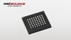
XC5VLX30 FPGA High-Performance Logic
Featured Product from Win Source Electronics
The XC5VLX30-1FFG676C combines high logic density with robust I/O support, providing engineers a powerful solution for mid-scale embedded systems and industrial applications. Built on 65nm CMOS and the second-generation ASMBL architecture, it delivers 4,800 slices (19,200 LUTs) and 1,152 Kbit Block RAM, giving designers ample resources to implement complex logic while maintaining efficient routing.
Thanks to its true 6-input LUT architecture, this FPGA enables dual 5-LUT output mode, supporting multifunctional roles such as distributed RAM or shift registers, maximizing resource reuse in compact designs. Its configurable on-chip memory with dual-port operation, optional ECC, byte-write capability, and FIFO logic is perfect for temporary storage, data buffering, or caching, which engineers often encounter in industrial automation and embedded control boards.
The XC5VLX30 also offers flexible I/O interface support, including LVTTL, LVCMOS, HSTL, SSTL, and LVDS, along with ChipSync™ source-synchronous interfacing and per-bit deskew, ideal for DDR memory, ADC interfaces, and other timing-sensitive signal applications. Coupled with advanced clock management via two CMTs, each with two DCMs and one PLL, the device ensures stable timing for critical operations such as multi-axis motion control or high-speed signal acquisition.
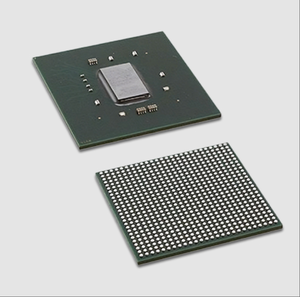
Packaged in a compact FFG676 (27×27mm) footprint, supporting up to 400 user I/Os, the XC5VLX30 balances I/O density with board routing flexibility, making it suitable for space-constrained systems and I/O-intensive modules. Its mature toolchain and long-term supply stability provide engineers with confidence in both development and production. For mid-scale embedded logic, industrial signal acquisition platforms, or general-pu