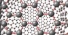
Nanoscale Materials

The construction of nanoparticle architectures on surfaces attracts substantial interest because of the degree of control that can be exercised over the size, shape and functions of the nanoparticle blocks and by their integration with bulk solid surfaces. The integration of functionalized metal nanoparticles with bulk conductive supports may lead to the electrical contacting of the nanoparticles and to the assembly of devices demonstrating single electron transfer charging devices or triggered electron transfer devices.4 ,242 The assembly of metal nanoparticles functionalized with recognition sites on electronic transducers such as electrodes or field-effect transistors may lead to new selective sensoric devices.243 ,244 Similarly, the assembly of nanoparticles on transparent surfaces or conductive transparent supports, may lead to controllable optical245 and electrochromic246 functionalities. For all of these functional systems the development of methods for the assembly and characterization of the nanoparticles on surfaces is essential. Several recent reviews have addressed this topic.6 ,7 ,42 The present section will briefly discuss the concepts for immobilization of metal nanoparticles on surfaces, and will exemplify the scientific methodologies of transforming the organized nanostructures into functional sensoric, electronic and photonic devices.
Monolayer deposition of functionalized nanoparticles onto a solid support surface is the first step for further multilayer functional assembly. Organized lattices, 2D- and 3D-ordered assemblies demonstrating sensoric, catalytic, electrochemical and photoelectro-chemical properties have been obtained. Nanosized electronic circuits were organized upon assembling of conductive metal...