III-Nitride Semiconductor Materials
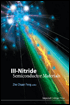
Written by renowned experts, this valuable resource covers the most important topics and achievements in recent years, discusses progress made by different groups, and suggests future directions.
 TABLE OF CONTENTS
 Vladimir Dmitriev and Alexander Usikov [*]
Technologies and Devices International, Inc.,
12214 Plum Orchard Dr., Silver Spring, MD 20904, USA
In this chapter we describe recent experimental results on hydride vapor phase epitaxy (HVPE) of group III nitride materials including epitaxial layers and multi-layer device structures. Properties of GaN, InN, AlN, and AlGaN layers grown by HVPE are presented. For GaN layers, n- type and p-type doping during HVPE growth is reported. Thick crack free AlN layers grown by stress control HVPE are described. New directions in HVPE technology including large area growth, multi-wafer growth, sub-micron multi-layer growth, and fabrication of nano-size structures including GaN and InN nanowires are briefly discussed. Properties of HVPE grown AlGaN/GaN hetero structures with two-dimensional electron and two dimensional hole gases are presented. Applications of HVPE grown group III nitride materials including substrate applications (template substrates, free standing substrates, and bulk substrates) and device structures for both optoelectronic application (blue and ultraviolet light emitting diodes grown by HVPE) and electronic applications (high electron mobility transistors grown by HVPE) are discussed as well.
The HVPE technology has been demonstrated to deposit single crystal layers of both GaN1 and AlN2 more than 30 years ago. Fig. 1 illustrates the basic idea of the method. For GaN growth, source materials are gallium chloride and ammonia gases. Gallium chloride is formed inside growth apparatus by a reaction of gaseous HCl and Ga metal. Formed gallium chloride is transported into a growth zone of the apparatus where it...