 Metrigraphics LLC is a leading worldwide supplier of ultra-high, precision,
custom components for Original Equipment Manufacturers (OEMs). They have applied
their core technologies of electroforming, photolithography, and thin-film sputtering to
help customers increase the performance, accuracy, and reliability of state-of-the-art
instruments and devices. Their process technologies are utilized in fabricating
complex 2-D and 3-D micro-components and micro-circuits used in medical,
biotechnology, telecommunications, semiconductor, industrial, and consumer markets.
Metrigraphics LLC is a leading worldwide supplier of ultra-high, precision,
custom components for Original Equipment Manufacturers (OEMs). They have applied
their core technologies of electroforming, photolithography, and thin-film sputtering to
help customers increase the performance, accuracy, and reliability of state-of-the-art
instruments and devices. Their process technologies are utilized in fabricating
complex 2-D and 3-D micro-components and micro-circuits used in medical,
biotechnology, telecommunications, semiconductor, industrial, and consumer markets.
Their primary areas of expertise are listed below.
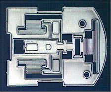
Through a combination of photolithography and their proprietary process technology, they can fabricate complex 2-D and
3-D micro-structures per the specific dimensional design specifications of their OEM customers. Micron size features at
sub-micron tolerances can be achieved in Au, Cu, NiCo, or Ni materials.
- High Density Flexible Circuits
High-resolution photolithography, thin-film coating, and micro-miniature 2-D and 3-D precision electroforming are combined to
produce high density, multi-layer flexible circuits with 5-micron traces and spaces. This technology allows medical product
designers to install communicating transmitters and transducers directly into intra-vascular, subcutaneous or implantable
devices for diagnostic imaging, monitoring or drug administration. High-density circuitry can be used inside devices with
diameters of only 1.25mm (e.g. catheters). A wide variety of in vivo and in vitro microcircuits have been produced in high
volumes on various substrates, including PZT, alumina, glass, and flexible polyimides.
- Micro-Nozzles/Orifice Plates
DRC provides electroforming apertures (≥ 1 micron) for nozzle and orifice plates used for precision jetting of liquids
and gases. Funnel-shaped and straight-walled apertures are available from this process for a wide variety of
microfluidic applications for medical and biological instruments and devices.
High aspect ratio micromechanical parts (gears, cams, springs and coils) are produced by electroforming,
ion beam etching, LIGA, and other processes.
- Precision Measurement and Control
They have applied precision electroforming to produce a wide variety of devices for control, test, and measurement
applications in medical and analytical instrumentation (e.g. spectrometers) on glass, quartz and other substrates,
both coated and non-coated. In applications where accuracy, repeatability and precision are critical, their engineers
have developed processes to produce key instrument components. Some products that they routinely supply are:
- Slits
- Grids
- Targets
- Reticles
|
- Gratings
- Encoder Scales
- Encoder Disks
- Other Optical Components
|
Precision patterns can be etched in almost any material up to a depth of a few microns using Ion Beam Etching. Depth-to-width
ratios can be as much as 5:1 and multi-layer metalizations are feasible. Pattern relief etching of dielectric substrates, such as
glass, is possible to precise depths of 10 angstroms!
- Thin Film Sputter Deposition
Using state-of-the-art sputter deposition equipment, they can deposit a very wide range of metals at Angstrom level thicknesses
on a wide range of substrate materials.
For more information on their products, please use one of the following links: