About
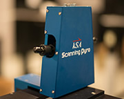
k-Space is a leading manufacturer of in situ, in-line, and ex situ metrology tools for the semiconductor, thin-film, and PV industries. Our tools are used for monitoring nearly all thin-film deposition processes, including MBE, MOCVD, PLD, PVD, sputtering, and evaporation. Our products utilize optical imaging technology for non-contact, non-invasive measurement of a plethora of important parameters.
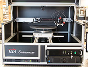
k-Space metrology tools focus on real-time data acquisition, processing, and analysis of nearly all deposition parameters of importance, including: wafer and film temperature, thin-film stress and strain, wafer curvature, bow, and tilt, surface roughness and quality, film thickness and deposition rate, optical band gap and atomic spacing. We also supply ex situ wafer and surface analysis tools which perform full curvature, stress, and wafer bow mapping on up to 300mm wafers.
Our tools are used in today's most advanced thin-film deposition and processing applications within compound semiconductor, silicon semiconductor and photovoltaic advanced thin film production and R&D. Sophisticated software analysis and reporting capabilities provide information to better understand tomorrow's electronic and optoelectronic devices or to provide online control during mass production to enhance yield. Tailored optics and fully integrated solutions have been designed for simple mounting and non-invasive monitoring of advanced deposition processes such as: MOCVD, MBE, sputtering, thermal and e-beam evaporation, and PLD.