A
semiconductor diode is a non-linear device whose most outstanding feature is
the fact that current is allowed to flow – basically – in one direction
only. The diode is built by joining
together two semiconductor materials: an N-Type material and a P-Type material. The area of contact is called thejunction. This is the reason why sometimes we refer to
the diode as a PN Junction.
When
an applied voltage forces the diode
to conduct we say that the diode is operating in the forward bias condition; when the supply voltage is connected such
that the current in the diode is minimal (practically zero) the diode is in the reverse bias condition. When in the forward bias mode1 the
diode behaves much like a closed switch; on the other hand, in reverse bias2 the diode behaves like an open switch. To understand the operation of a diode we must understand the diode I-V
characteristics.
Diode
Characteristics
Figure
5.1 shows the typical I-V characteristics of a silicon
diode3. The two operating
regions are clearly labeled. Notice the
different scales used to indicate the current in each case. For the forward bias case the current in the
particular I-V curve is expressed in milli-amps (mA), whereas in the reverse bias region the current is
expressed in micro-amps (µA). The main
features of these two operating conditions are explained below.
Forward Bias Region
As
you can see, at low levels of diode voltage the current is very small. After reaching a particular voltage – called
the threshold voltage, or Vthr –
the current increases abruptly. The
threshold voltage is dependent on the type of material the diode is built
with: For a Silicon diode the
Vthr = 0.7 V, and for a Germanium diode Vthr = 0.3 V.
In
the forward bias region we can distinguish two important areas in relation to
the amount of current in the diode.
Diode Voltage is≤VthrFor any diode voltage (VD) between zero and Vthr the current is
very small. In general, as an
approximation, we may consider this current to be zero. This means that in this range the diode
behaves like an open circuit, or like a device with a very high resistance.
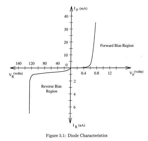
Diode Voltage≥Vthr In this region the current increases very fast. As you can see in Fig. 5.1 the voltage across the diode (VD) remains more or less
constant and equal to Vthtr. In this area the diode voltage is independent
of the source voltage. Sometimes we
assume that the diode voltage is equal to zero, so the diode behaves like a
closed switch, or like a device with a very small resistance.
1And the junction voltage is bigger than the threshold voltage – approximately 0.7 V for Silicon diodes and 0.3 V for Germanium diodes.
2And when the junction voltage is less than the breakdown voltage.
3See Experiment No. 2 for general considerations of characteristics of non-linear devices.
Reverse Bias Region
In
reverse bias the current through the diode is very small (practically zero)
when the junction voltage is between zero and the so-called breakdown voltage, VBD. This is the
voltage that produces an abrupt increase in current. The breakdown voltage is not a constant value
like the threshold voltage in forward bias. VBD is different
for each diode. This value is a
specification parameter given by the manufacturer.
Like
in the last case, in reverse bias we can distinguish two important areas.
Diode
Voltage is≤VBD In this area the current is very small. We call this current the leakage
current. In practical applications
you may consider it to be zero. Thus, in
this area the diode behaves like an open switch, or like a device with a very
large resistance.
Diode
Voltage is≥VBD In the breakdown region the current increases very fast as a function of the
diode voltage. The diode behaves like a
closed switch, or like a device with a very small resistance. Notice that the diode voltage in this case is
very close to VBD for
practical applications, for any source voltage.
| Current
| Resistance
| Ideal
Behavior
|
Forward Bias
(VD ≤ Vthr)
| ≈ 0
| very large
(≈∞)
| open switch
|
Forward Bias
(VD ≥ Vthr)
| large
| very small
| closed switch
|
Reverse Bias
(VD ≤ VBD)
| ≈ 0
| very large
(≈∞)
| open switch
|
Reverse Bias
(VD ≥ VBD)
| large
| very small
| closed switch
|
Table
5.1: Diode Conditions
Table
5.1 is a summary of the diode operating conditions. The last column of the table indicates the
behavior of an ideal diode. When an
ideal diode is forward biased it would behave like a closed switch with a
resistance equal to zero ( 0 Ω). In reverse bias the ideal diode is similar to
an open switch with current equal to zero and infinite (∞ Ω)
resistance.
Note:
Of course ideal diodes do not exist,
so the forward resistance of the diode is not 0 Ω but a low resistance,
and the reverse bias resistance is not ∞ Ω but a high resistance.
Diode
Identification
The
schematic symbol for the diode is typically a filled arrow with a short line
across the tip. The cathode is the N-type material and is represented by the tip of
the arrow. The anode is the P-type material and is indicated by the base of
the arrow.
The
manufacturers of diodes used diverse methods to indicate the anode and the
cathode. In the most common method the
cathode (N-type material) is usually identified with a colored band. Thus, the end of the diode closest to this
band is the cathode. The other end is
the anode (P-type material.)
Connections
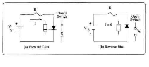
Figure 5.2: Diode Biasing: Forward and Reverse
When
a diode is used in a completed circuit, if the positive potential (highest) is
connected to the P material and the negative potential to the N material, then
the diode is in forward bias. If, on the
other hand, the highest potential is connected to the N material and the lowest
potential to the P material (or, in other words, if the N material is at higher
potential than the P material) the diode is reverse biased. Figure
5.2 shows the forward and reverse biasing of a diode (ideal, in the case)
connected to a circuit. The student
should pay special attention to the connections needed to achieve a particular
biasing.
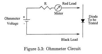
Ohmmeter Measurement
To
find the condition of a diode we can measure its resistance with an
ohmmeter. The actual resistance can be
measured, but the student should be aware that this process is often a source
of some confusion.
The
equivalent circuit of an ohmmeter is shown in Figure 5.3. The meter movement may be represented as some
resistance which could be lumped with the ohmmeter resistance R, as shown in the figure. If we connect the test lead of the meter as
shown, the circuit is really a simple forward biased circuit as shown in Figure
5.3. What causes the confusion is that
the equivalent voltage varies from one meter to another and even changes
whenever the ohmmeter’s range is changed. This varies the amount of forward biasing applied to the diode, and as a
consequence varies the resistance measurement, so the same diode might measure
a forward resistance, say, of 20 Ω on one range and 300 Ω on another range or on
another meter. This is quite normal and,
once understood, will not bother the student.
The
important things that must be known when taking the resistance measurements
concern the ohmmeter’s test lead polarity, and the ratio of forward and reverse
diode resistance. The student should
test the ohmmeter with a voltmeter to be sure of the test lead polarity, or else
refer to the operating manual for the instrument. The actual measured forward or reverse
resistance of a diode is not particularly important. What is important is that the resistance
should be much higher in one direction than in the other, typically 1 kΩ or
less in the forward bias direction and 1 MΩ in
the reverse direction. The measurement
of any semiconductor resistance will always depend upon the ohmmeter’s internal
voltage.
© 2026 GlobalSpec, Inc.
 This book is designed for students who are taking their first course in analog electronics in either a two-year or four-year program. The prerequisites are a DC-AC course; a basic knowledge of algebra, including the ability to solve simultaneous linear equations; and a strong knowledge of trigonometry. The main topics in this book provide an introduction to the most important semiconductor devices: how they are built, how they operate, and how they are used in larger electronic modules.