Besides
the PN diodes that we studied in the last experiment there are many more types
of diodes. Each one is used in
applications that can take advantage of its behavior and characteristics. What follows is a short statement explaining
features of some of these special purpose diodes.
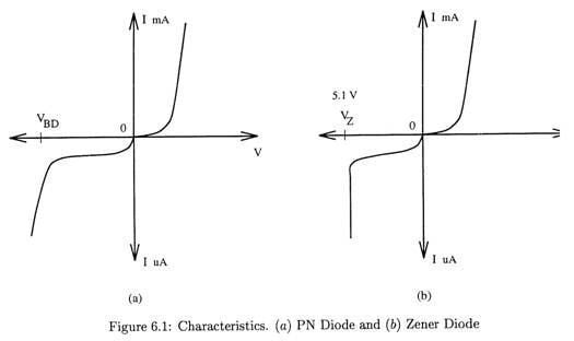
Zener Diode
A zener diode is similar to the PN diode, but with special
fabrication techniques it can be built with a specific
breakdown
voltage. The breakdown voltage of these
diodes is called the Zener voltage, VZ. A typical PN diode normally
has a very large breakdown voltage. A zener diode, on the other hand, can have practically any value for the
breakdown voltage. You can find zener
diodes with VZ ranging from a few volts to several hundred
volts. Another important feature that
makes the zener diode different from the normal PN diode is that at breakdown
the characteristic curve is approximately a vertical line, indicating that in
breakdown the Zener diode produces nearly constant voltage. Thus a Zener diode operating in its breakdown
region will produce a constant voltage equal to VZ. Because of this fact, the Zener diode is
normally used in the reverse-bias direction. Figure 6.1 shows the characteristic curves of a typical PN diode and a
typical Zener diode with VZ = 5.1 V. Notice the difference in the breakdown regions of both devices.
LED
The
Light-Emitting Diode (LED) produces light when forward biased. In the LED the electrical energy applied to
the junction raises the energy level of the electrons. As they return to their original energy
level, they emit photons (light particles). The light is visible. The LED is one of most versatile
electro-optical devices, forming the displays of practically all electronic
devices such as VCR’s, clock receivers, TV sets, remote controls, etc.
LEDs light up when forward
biased. The typical forward voltage (VF) and forward current (IF) for LEDs are as follows:

IF : < 20 mA
for AC operation and < 10 mA for
DC operation.
Caution:
LEDs typically have reverse
breakdown voltage of the order of 5V. This means you must be very careful not to use LEDs with a high level
of reverse bias because the current could be very high.
The
color of the light given off by an LED depends on the material used in its
construction and on the construction technique.
Schottky Diode
The standard PN
diodes are built with P- and N-type material.
The Schottky diode is constructed by
bending a metal (aluminum or platinum) to, for example, N-type silicon. In other words we form the diode’s anode with
metal rather than with P-type material. The threshold voltage (Von)
of the Schottky diode is around 0.3V like the germanium diode.
The characteristic behavior of this
diode is very similar to the characteristic of the standard PN diode. The main difference is the fact that the
Schottky diode can switch ON and OFF much faster than the PN junction
diodes. Another difference is that the
Schottky diode produces less unwanted noise than either the silicon or
germanium diodes. These two
characteristics make the Schottky diode very useful for applications where
high-speed switching power circuits are required.
The Schottky diode and the germanium
diode have both the same turn-on voltage, as we have seen (0.3V). The Schottky diode, however, has the
additional advantage of speed. As a result,
you rarely see a germanium diode in use today.
Figure 6.2 shows the layout of the
construction of this diode, the symbol, and a typical characteristic
curve. Notice that there is only one
semiconductor piece (the N-type material). The anode side of the Schottky diode is a piece of metal, as you can
see.

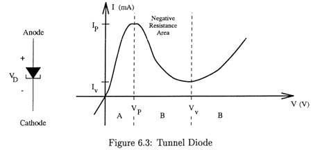
Tunnel Diode
These type of diodes have the unique feature that for
a particular voltage range they act as a negative
resistance! Figure 6.3 shows the
symbol used to represent the tunnel diode and a typical characteristic curve.
In
the I-V curve we can distinguish three important regions: In regions A and C the diode behaves like a
typical device with positive resistance; this means that as the voltage
increases the current will increase as well. In the second region (region B), however, you can see that as the
voltage increases, between VP and Vu, the current
decreases.
Negative
resistances are useful in oscillator construction and in high frequency
applications, and this is where sometimes you will find a tunnel diode.
Note:
The negative resistance of the tunnel
diode only manifests itself for AC signals. For DC, a positive voltage will produce a positive current.
Varactors
As you know, when a PN diode is biased
by applying a voltage to the junction the physics of the device results in a
negative charge on the P side and positive charge on the N side. The region these positive and negative
charges form, known as the depletion region,
does not contain any moving charges.
The result of the above statements is that
we end up with charges separated by an insulator. This is exactly a capacitor.
In fact, all PN junctions have an associated
capacitance (Cj). When voltage is applied to the diode, the
depletion region decreases (forward bias) or increases (reverse bias), changing
the value of the PN junction capacitance.
Some diodes are specially manufactured so
that the PN junction capacitance has a known and controllable relation to the
applied diode voltage. This produces a
device known as a varactor, which
has a voltage controlled capacitance. These diodes are operated normally in reverse bias only. Figure 6.4 shows the layout, the symbol, and
the curve that shows the relationship between the applied reverse bias voltage
and the capacitance.

Note
that the reverse bias voltage (VR)
increases the capacitance decreases. The
quality CT is the
capacitance of the device when there is no applied voltage. The relation between the reverse bias voltage
and the capacitance is given by the following formula.

Notes:-
For some varactors the denominator of the above
equation is cube root rather than a square root.
-
The useful range of the varactor is
approximately 1/2 to 1/3 of the zero-bias value (Cj).
Photo Diodes
A photo diode converts light energy into electrical energy. Devices that convert from one form of energy
to another are known as transducers,
sensors, or detectors.
The photo diode works as
follows: You know that the reverse bias
current of a diode is very small. If we
can construct a diode so that light (photons) can reach the junction, then the
energy imparted by the photons to the atoms in the junction will create more
free electrons (and more holes). These
extra electrons will create a large reverse bias current. As the incident light is increased, the
reverse-bias current increases.
If we use the photo diode in reverse
bias, then we have a device that its current output is dependent on the
intensity of the incident light. Used in
this fashion, the photo diode is operating in the photoconductive mode. If we
use the photo diode in the forward bias region, we have a device that produces
an output voltage in response to light illumination; used in this manner, the
photo diode is operating in the photovoltaic
mode.
Note:
It is not the purpose of this experiment
to study photo diodes in particular. To
know more about this topic, the reader should read any introductory electronic
book.
Figure
6.5 shows the symbols used for the different diodes that we have presented
here.

© 2026 GlobalSpec, Inc.
 This book is designed for students who are taking their first course in analog electronics in either a two-year or four-year program. The prerequisites are a DC-AC course; a basic knowledge of algebra, including the ability to solve simultaneous linear equations; and a strong knowledge of trigonometry. The main topics in this book provide an introduction to the most important semiconductor devices: how they are built, how they operate, and how they are used in larger electronic modules.