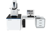
Ultra-High Resolution FE-SEM: SEM5000X
Featured Product from CIQTEK Co., Ltd
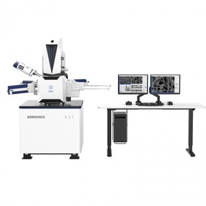
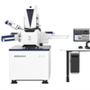
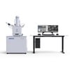
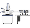
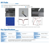
The SEM5000X redefines imaging precision with its groundbreaking 0.6 nm resolution at 15 kV and 1.0 nm at 1 kV, setting new standards in electron microscopy. Leveraging advanced "Super Tunnel" technology and precision engineering, this FE-SEM ensures exceptional clarity even at low voltages. With 16 specimen chamber ports and support for up to 8-inch wafers, including a maximum diameter of 208 mm, it provides expansive coverage for metallurgical and semiconductor applications. Enhanced scanning modes and automated functions further elevate performance, promising an unparalleled user experience.
Highlighted Features and Applications:
- Ultra-High Resolution: Achieves an unprecedented 0.6 nm resolution at 15 kV, opening new frontiers in imaging accuracy.
- Versatile Compatibility: Supports a wide range of applications, including metallurgical and semiconductor analysis.
- Enhanced Automation: Advanced scanning modes and automated functions streamline workflows, enhancing productivity.
- Expanded Coverage: With 16 specimen chamber ports and support for up to 8-inch wafers, it accommodates diverse sample sizes, enabling comprehensive research and analysis.