Semiconductor Electrostatic Chucks
Featured Product from Fountyl Technologies Pte. Ltd.
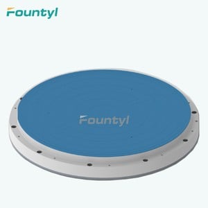
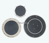
These state-of-the-art Semiconductor Electrostatic Chucks (ESCs) deliver exceptional clamping uniformity and stability. Engineered with high-purity ceramic materials (AlN/Al2O3), they provide reliable performance across ultra-high vacuum and high-temperature manufacturing environments.
Key Technical Features
Multi-Zone Thermal Control: Advanced multi-zone cooling profiles achieve precise temperature uniformity across the entire wafer surface.
Rapid Chucking & Dechucking: Optimized transient response times with minimized residual charge boost manufacturing throughput.
High Corrosion Resistance: Proprietary coating technologies withstand aggressive plasma chemistries to significantly extend component lifespan.
Target Applications
The ESC design is fully optimized for critical steps in semiconductor fabrication, including:
Plasma Etching: Conductor, dielectric, and polysilicon etch processes.
Chemical Vapor Deposition (CVD): High-temperature PECVD and ALD systems.
Physical Vapor Deposition (PVD): Sputtering processes requiring strict thermal management.
Ion Implantation: High-dose and low-energy implantation systems.
Industry Value
Maximized Die Yield: Eliminates wafer backside particle contamination and reduces detrimental thermal stress.
Lowered Cost of Ownership (CoO): Extended operational lifetimes drastically reduce tool downtime and maintenance frequency.
Next-Gen Node Readiness: Proven performance for advanced sub-3nm nodes and high-aspect-ratio features.