Silicon Carbide Wafer Pin Chuck
Featured Product from Fountyl Technologies Pte. Ltd.

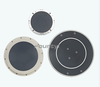
High-Performance Wafer Pin SiC Chuck for Semiconductor Equipment
The silicon carbide wafer pin chuck—also known as a prealigner chuck—is engineered for precision wafer handling in semiconductor manufacturing. Made from high-performance materials like silicon carbide or alumina ceramic, this chuck offers exceptional heat, corrosion, and wear resistance. Its pin-type structure enhances adsorption strength, reduces contamination, and ensures reliable wafer positioning.
Key Features:
-
High temperature resistance: Maintains stability and shape under long-term exposure to elevated temperatures without deformation or breakage.
-
Excellent corrosion resistance: Ideal for chemically harsh environments, withstanding corrosive gases and liquids.
-
Outstanding wear resistance: High hardness ensures long service life and reliability in repetitive wafer processing.
-
Pin-point adsorption structure: Raised pin design minimizes contact area while maximizing unit adsorption force—ensuring secure wafer fixation.
-
Enhanced cleanliness and stability: Evolution from groove-type to pin-type chucks reduces particle contamination and improves wafer flatness correction.
-
Precision control: Supports 12-inch wafers with flatness ≤ 5 μm; customizable for more stringent accuracy needs.
-
Shape adaptability: Wafer clamping shape and pin pattern can be adjusted according to wafer geometry for optimal handling.
-
Material options: Choose between silicon carbide or alumina ceramic; optional surface coatings include DLC and Teflon for added protection.
-
Flexible applications: Suitable for wafer exposure, inspection, and transfer processes requiring superior stability and durability.
Applications:
-
Wafer clamping in semiconductor exposure tools
-
Wafer fixation in inspection and metrology equipment
-
High-precision wafer handling in transfer and alignment systems
This chuck is designed to help semiconductor engineers and equipment manufacturers achieve better wafer flatness control, reduce yield loss due to contamination, and maintain performance in the most demanding fabrication environments. Custom solutions are available to meet your specific process needs.