
-
Supplier: Renesas Electronics Corporation
Description: may be over-driven by an external clock. The “LV” terminal may be tied to GND to bypass the internal series regulator and improve low voltage (LV) operation. At medium to high voltages (3.5V to 12V), the LV pin is left floating to prevent device
- Output Voltage (Volt): 1.5 to 22.8 volts
- Input Voltage (VIN): 1.5 to 12 volts
- Features: Other
- Package Type: SOIC / SOP
-
Supplier: Integrated Device Technology
Description: The 508 is the most cost effective way to generate a high quality, high frequency CMOS clock output from a PECL clock input. The 508 has separate VDD supplies for the PECL input buffer and the output buffer, allowing different voltages to be used. For example, the
- TJ: 0 to 70 C
- Pin Count: 8 #
- Supply Voltage: 3.3 V, 5 V
- Device Type: Buffer
-
Supplier: Renesas Electronics Corporation
Description: may be over-driven by an external clock. The “LV” terminal may be tied to GND to bypass the internal series regulator and improve low voltage (LV) operation. At medium to high voltages (3.5V to 12V), the LV pin is left floating to prevent device
- Output Voltage (Volt): 1.5 to 22.8 volts
- Input Voltage (VIN): 1.5 to 12 volts
- Features: Other
- Package Type: SOIC / SOP
-
-
Supplier: Microchip Technology, Inc.
Description: The TC7662A is a pin-compatible upgrade to the Industry standard TC7660 charge pump voltage converter. It converts a +3V to +18V input to a corresponding –3V to –18V output using only two low-cost capacitors, eliminating inductors and their associated cost,
- Features: Other
-
Supplier: Richardson RFPD
Description: The AD7656/AD7657/AD7658 contain six 16-/14-/12-bit, fast, low power, successive approximation ADCs all in the one package that is designed on the iCMOS™ process (industrial CMOS). iCMOS is a process combining high voltage silicon with submicron CMOS and complementary bipolar
- Resolution: 12 bits
- Sample Rate: 250 kSamples/Sec
- Package Type: QFP
-
Supplier: Daburn Electronics & Cable
Description: Frequency: 100 KHz min. Protection: Short Circuit Protection Over Voltage Protection REMOTE ON/OFF CONTROL (Optional) Control Voltage Referenced To Negative (-) Input Compatibility: CMOS, TTL On Control: 4.8V min. on open Off Control: 0-1.8V max. on short Logic
- DC Input Voltage: 5 to 48 volts
- DC Input Current: 0.01 to 2.47 amps
- DC Output Voltage: -3.3 to 3.3 volts
- DC Output Current: 3 amps
-
Supplier: Daburn Electronics & Cable
Description: Our 8 watt single and dual output DC-DC converter features a five-sided EMI shield and no derating up to 70°C. It has an efficiency of 80% and a minimum input/output isolation of 1500 Vdc. INPUT Input Voltage: Voltage Range 12 Vdc: 9 - 18 Vdc 24 Vdc: 18 - 36 Vdc 48 Vdc:
- DC Input Voltage: 12 to 48 volts
- DC Output Voltage: -15 to 15 volts
- DC Output Current: 0.8 to 2 amps
- DC Output Power: 8.00000000000003 watts
-
Supplier: Daburn Electronics & Cable
Description: Response, 25% load step: 500 mS Transient Voltage Peak Deviation: 1% of Vout REMOTE ON/OFF CONTROL Control Voltage Reference to Negative (-) Input Compatability: CMOS, TTL On Control: 4.8V min. or Open Off Control: 0.4V max. or Short GENERAL Efficiency: Up to 91%
- DC Input Voltage: 12 to 48 volts
- DC Output Voltage: 1.5 to 15 volts
- DC Output Current: 2 to 6 amps
- DC Output Power: 30.000000000000004 watts
-
Supplier: Renesas Electronics Corporation
Description: excellent frequency domain performance are achieved using a segmented architecture. The digital inputs are TTL/CMOS compatible and translated internally to ECL. All internal logic is implemented in ECL to achieve high switching speed with low noise. The addition of laser
- Resolution: 12 bits
- DNL: 1 LSB
- INL: 1.5 LSB
- Package Type: SOIC
-
Supplier: Cirrus Logic, Inc.
Description: voltage-to-frequency converters and multislope integrating A/D converters Differential inputs Single-channel (CS5507/08) and 4-channel (CS5505/06) pseudo-differential versions Either 3.3 V or 5 V digital interface Linearity error ±0.0015% FS (16-bit CS5505/07)
- Resolution: 20 bits
- Package Type: SOIC
- ADC Type: Sigma-Delta
-
Supplier: Microchip Technology, Inc.
Description: The TC962 is an advanced version of the industry-standard 7662 high-voltage DC-to-DC converter. Using improved design techniques and CMOS construction, the TC962 can source as much as 80mA versus the 7662 ’s 20mA capability. As an inverter,the TC962 can put out
- Operating Temperature: -45 to 85 C
- Configuration / Function: Charge Pump
- Package Type: DIP / CDIP / PDIP, SOIC / SOP
- Features: Other
-
Supplier: Daburn Electronics & Cable
Description: and Triple: 10% REMOTE ON/OFF CONTROL Control Voltage Reference to Negative (-) Input Compatibility: CMOS, TTL On Control: 4.8V min. or Open Off Control: 0.4V max. or Short GENERAL Efficiency: 84 - 90% Isolation Voltage: 1600 Vdc min. Isolation Resistance: 1000 MOhms
- DC Input Voltage: 24 to 48 volts
- DC Output Power: 40 watts
- Number of Outputs: 1 to 3 #
- Form Factor: Board Mount
-
Supplier: ACCES I/O Products, Inc.
Description: can be used as an A/D pacer clock and/or can be used to measure pulse width, count events, measure or generate frequencies, etc. An on-board 1 MHz crystal controlled clock is hard-wired to one counter input and the clock inputs to the other two counters are available at the I/O
- Analog Input Channels: 8 #
- Operating Temperature: 32 to 140 F
- Resolution: 12 bits
- Features: Analog-to-Digital Converter, DC Voltage Input, ISA / EISA
-
Supplier: Infineon Technologies AG
Description: response in active burst mode 65kHz internally fixed switching frequency Auto restart protection mode for overload, open loop, V CC under voltage, over temperature & over voltage Built-in soft start Built-in blanking window with extendable blanking time for short duration high
- Output Power: 39 watts
- Operating Temperature: -40 to 130 C
- Configuration / Function: Flyback Converter
- Features: Other
-
Supplier: Microchip Technology, Inc.
Description: panel. The MIC4832 is offered in MSOP-8 lead-free and RoHS-compliant packaging with a -40°C to 85°C junction temperature range. Additional Features 1.8V to 5.5V DC input voltage 220VPP output voltage capable Low audible noise EL drive waveform Supports EL panel sizes up
- Features: Other
-
Supplier: Richardson RFPD
Description: The ADL6317 is a transmit variable gain amplifier (VGA) that provides an interface from radio frequency digital-to-analog converters (RF DACs), transceivers, and systems on a chip (SoC) to power amplifiers. Integrated balun and hybrid couplers allow high performance RF
- Frequency Range: 1,500 to 3,000 MHz
- Features: Other
-
Supplier: Richardson RFPD
Description: The ADRF6650 is a highly integrated downconverter that integrates dual mixers, dual digital switched attenuators, dual digital variable gain amplifiers, a phase-locked loop (PLL), and voltage controlled oscillators (VCOs). In addition, the ADRF6650 integrates two radio frequency (RF)
- Input Frequency Range: 450 to 2,700 MHz
- Output Frequency Range: 450 to 2,900 MHz
- Conversion Gain: 29 dB
- Noise Figure: 11 dB
-
Supplier: Renesas Electronics Corporation
Description: The EL7554 is a full-feature synchronous 4A step-down regulator capable of up to 96% efficiency. This device operates from 3V to 6V VIN input supply. With internal CMOS power FETs, the device can operate at up to 100% duty ratio, allowing for output voltage range
- Regulated Output Voltage (Volt): 0.8 to 6 volts
- Output Current (IOUT): 4 amps
- Quiescent Current (IQ): 0.001 amps
- Input Voltage (VIN): 3 to 6 volts
-
Supplier: Richardson RFPD
Description: the converters to maintain excellent performance.The ADC output data can be routed directly to the two external 16-bit output ports or multiplexed on a single 16-bit bus. These outputs can be set to either 1.8 V CMOS or LVDS. Flexible power-down options allow
- Category: Development Board
-
Supplier: Microchip Technology, Inc.
Description: The TC426/TC427/TC428 are dual CMOS high-speed drivers. A TTL/CMOS input voltage level is translated into a rail-to-rail output voltage level swing. The CMOS output is within 25mV of ground or positive supply. The low impedance, high-current driver outputs
- Features: MOSFET
-
Supplier: Infineon Technologies AG
Description: output voltage with secondary side control regulation. Besides having the basic features of the F3R CoolSET™ such as Active Burst Mode, propagation delay compensation, soft gate drive, auto restart protection for major fault (Vcc over voltage, Vcc under voltage, over
- Category: Development Board
-
Supplier: Nexperia B.V.
Description: voltage, provided by an internal voltage regulator, is used to supply circuitry in signal paths controlling the low-side and high-side power switches. This enables a low-power operation and a better controlled driver performance irrespective of the IC supply voltage.
- IC Package Type: Other
-
Supplier: Infineon Technologies AG
Description: Operating/Switching Frequency (50kHz - 250kHz) Max Duty Cycle of 95% (at 25°C) at 125kHz Trimmed Internal Reference Voltage (3V+2% at 25°C) VCC Under-Voltage Lockout Cycle by Cycle Peak Current Limiting Output Over-Voltage Protection Open Loop Detection Enhanced Dynamic
- Quiescent Current (IQ): 0.0003 amps
- Operating Temperature: -40 to 125 C
- Features: Other
-
Supplier: Laurel Electronics LLC
Description: Intertek #4006497 RoHS 3 Compliant CE Certificate Features 0.2, 2, 20, 200, 300 & 600V AC or AC+DC voltage ranges 2, 20, 200 mA & 5A AC or AC+DC current ranges Accuracy to 0.03% of full scale, 0.1% to 100% of FS, 10 Hz to 5 kHz 0.03% accuracy of full scale at crest factor
- Number of Digits: 5
- Width: 118.872 mm
- Height: 62.23 mm
- Depth: 143.256 mm
-
Supplier: Laurel Electronics LLC
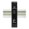
Description: The analog input batch controller utilizes the Laureate VF voltage-to-frequency converter signal conditioner board, which converts 4-20 mA, 0-1 mA or 0-1V conditioned flow meter signals to a frequency from 10 kHz to 110 kHz. This allows the counter
- Operating Temperature: -40 to 158 F
- Functions: Batch Counter
- Mounting: DIN Rail Mount
- Signal Input Type: Frequency / Pulse
-
Supplier: Laurel Electronics LLC
Description: input batch controller utilizes the Laureate VF voltage-to-frequency converter signal conditioner board, which converts 4-20 mA, 0-1 mA or 0-1V conditioned flow meter signals to a frequency from 10 kHz to 110 kHz. This allows the counter controller
- Operating Temperature: -40 to 158 F
- Functions: Batch Counter
- Mounting: DIN Rail Mount
- Signal Input Type: Frequency / Pulse
-
Supplier: ACCES I/O Products, Inc.
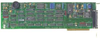
Description: generation. Also, Counter/Timers 1 and 2 can be jumper programmed to initiate A/D conversions. ANALOG OUTPUT The card has two multiplying 12-bit digital-to-analog converters (D/A) connected to output drivers capable of providing 5 mA current drive. Each channel provides
- Analog Input Channels: 16 #
- Digital I/O Channels: 8 #
- Sampling Frequency: 50 kHz
- Resolution: 12 bits
-
Supplier: ValueTronics International, Inc.
Description: MHz to 25 MHz: -45 dBc Square/Pulse Characteristics Frequency: 1 µHz to 10 MHz Duty Cycle: 20% to 80% Rise/Fall Time: < 24 ns (10% to 90%) Overshoot (1 kHz, 1 Vpp Typical): < 3% Pulse Width: > 50 ns Jitter: < 500 ps + 10 ppm Ramp Characteristics Frequency: 1
- Bandwidth: 200 MHz
-
Supplier: Laurel Electronics LLC
Description: voltage-to-frequency signal conditioner board can be scaled to display rate or totalized rate to six digits for 0-1 mA, 4-20 mA or 0-10V analog process signals to a frequency of 10 kHz to 110 kHz. Special input ranges are available from the
- Number of Digits: 6
- Width: 118.872 mm
- Height: 62.23 mm
- Depth: 143.256 mm
-
Supplier: ValueTronics International, Inc.
Description: analog-to-digital converter (ADC) to convert the voltages it measures into digital information. Additional Features: 150 MHz frequency bandwidth and a maximum of 8 full-range input channels 250 MS/s channel-by-channel A/D converters, providing a maximum
- Bandwidth: 150 MHz
- Number of Input Channels: 8 (# channels)
-
Supplier: Infineon Technologies AG
Description: ±5% tolerance Over-current detection with negative voltage input Single pin for fault output and enable Programmable fault clear time Wide supply voltage rage with 25 V VCC max Under voltage lockout for IGBTs CMOS Schmitt-triggered inputs 3.3 V, 5 V and 15 V input logic
- Peak Output Current: 2.6 amps
- Supply Voltage: 12.7 to 20 volts
- Propagation Delay: 50 ns
- Driver Type: Low-side Gate Driver
-
Supplier: ValueTronics International, Inc.
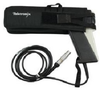
Description: effect technology to provide broad bandwidth measurement capabilities from DC up to 100 MHz at current levels as low as 1 milliamp to thousands of amps (when used with CT4 current transformer). When connected to Tektronix TDS Oscilloscopes with TEKPROBE Level II or
- Bandwidth: 15 MHz
- Probe Type: Current










Find Suppliers by Category Top
Featured Products Top
-
 The ALD4213 quad SPST CMOS analog switches from Advanced Linear Devices offer fast switching, low on-resistance, micropower consumption, and excellent precision for low-voltage and high-speed applications. These switches are specifically designed for use in (read more)
Browse IC Analog Switches Datasheets for Advanced Linear Devices, Inc. -
The ALD2706 from Advance Linear Devices is a dual monolithic CMOS operational amplifier (op-amp), optimized for a broad range of analog applications. It offers rail-to-rail I/O voltage ranges and draws max 80µA at 5V. The op amp is designed for +5V (read more)
Browse Operational Amplifiers Datasheets for Advanced Linear Devices, Inc. -
analog semiconductors, specializing in the development and manufacture of precision CMOS linear integrated circuits, including analog switches, A/D converters and chipsets, voltage comparators, operational amplifiers, energy harvesting systems, analog timers, and conventional and precision EPAD MOSFET transistors. For more information about Advanced Linear Devices go to www.aldinc.com. (read more)
Browse Uncategorized Products Datasheets for Advanced Linear Devices, Inc. -
complementary ALD1105, and it can be used to construct CMOS analog switches when connected in parallel with sources, drains, and gates connected together. It is also intended as a building block for CMOS inverters, differential amplifier input stages, transmission gates, and multiplexer applications (read more)
Browse Metal-Oxide Semiconductor FET (MOSFET) Datasheets for Advanced Linear Devices, Inc. -
-channel offset, gain, and phase adjustment provide the ability to calibrate and remove system-level errors upstream to the DAS. The AD4854 features a serial peripheral interface (SPI) register configuration bus (0.9 V to 5.25 V) and supports both low-voltage differential signaling (read more)
Browse Analog-to-Digital Converter (ADC) Chips Datasheets for DigiKey -
, Inc. Advanced Linear Devices, Inc. (ALD) is a design innovation leader in analog semiconductors specializing in the development and manufacture of precision CMOS linear integrated circuits, including analog switches, A/D converters and chipsets, voltage comparators, operational (read more)
Browse Metal-Oxide Semiconductor FET (MOSFET) Datasheets for Advanced Linear Devices, Inc.
More Information Top
 Indicates content that may require registration and/or purchase.

-
On-Chip Power Delivery and Management
A. Djemouai, M. Sawan, M. Slamani, High performance integrated CMOS frequency to voltage converter , in Proceedings of the International Conference on Microelectronics, pp. 63–66, Dec 1998 402.
-
An enhanced pulse width modulator with adaptive duty cycle and frequency control
and M. Slamani, “High Performance Integrated CMOS Frequency to Voltage Converter ,” Proceedings of the IEEE International Conference on Microelectronics, pp. 63-66 , December 1998.
-
Clock duty cycle adjuster circuit for switched capacitor circuits
Symp.on VLSI Circuits, Honolulu, Hawaii,USA, June 1996, pp. 142-143 DJEMOUAI,A,, et al.: ‘High performance integrated CMOS frequency to voltage converter ’.
-
Low power Schmitt trigger circuit
Symp.on VLSI Circuits, Honolulu, Hawaii,USA, June 1996, pp. 142-143 DJEMOUAI,A,, et al.: ‘High performance integrated CMOS frequency to voltage converter ’.
-
A 200 MHz frequency-locked loop based on new frequency-to-voltage converters approach
In this paper, we propose a high frequency, fully integrated frequency-locked loop (FLL) design based on a new architecture of a CMOS frequency - to - voltage converter .
-
Advanced Electrical and Electronics Engineering
Djemouai, A., Sawan, M., Slamani, M.: High performance integrated CMOS frequen- cy - to - voltage converter .
-
A new controlled gain phase-locked loop technique
High Performance Integrated CMOS Frequency - to - Voltage Converter ”.
-
New circuit techniques based on a high performance frequency-to-voltage converter
In the present paper, we presented a new design of a CMOS frequency - to - voltage converter .
-
Information Technology Applications in Industry
[3] Abdelouahab Djemouai, Mohamad A.Sawan et al, New Frequency-Locked Loop Based on CMOS Frequency - to - Voltage Converter : Design and Implementation, IEEE Transac-tions on Circuits and System-Ⅱ:Analog and Digital Signal Processing, Vol.48, No.5,May,2001:441…
-
A single capacitor loop filter phase-locked loop with frequency voltage converter
New frequency-locked loop based on CMOS frequency - to - voltage converter : Design and implementation.