
Products & Services
See also: Categories | Featured Products | Technical Articles | More Information-
Supplier: DigiKey
Description: KIT ETCHING PCB ECONOMY W/PUMP
-
Supplier: LPKF Laser & Electronics North America
Description: S to visually inspect and properly align the material. Circuit traces as small as 100 µm (4 mil) can be achieved with laminated PCB materials and 50 µm traces can be achieved, along with spacing of 25 µm when working with ceramics. Smaller features may be possible and results are dependent on
- X-axis Travel / Length Capacity: 9 inch
- Y-axis Travel / Width Capacity: 12 inch
- Z-axis / Vertical Travel: 0.4 inch
- Type: Complete / Turnkey System
-
Supplier: Technic, Inc.
Description: chemistry and equipment. Applications Base and precious metals plating Copper flash plate, panel plate, pattern plate Developing, etching, stripping Chemical cleaning MP100 Advantages Edge-to-edge processing forms a continuous flow through the plating cell eliminating edge effects and
- Machinery Type: Continuous Web - Reel to Reel
- Process / Technology: Electroplating
- Application / Industry: Printed Circuit Boards (PCB)
-
-
Supplier: FX PCB Co., Ltd.
Description: but it was not until the 1950s that they began to be used extensively in electronic equipment. Today, PCBs are found in almost all electronic devices, from simple calculators to complex computers and telecommunications equipment. PCB Manufacturing Process To make
- Features: East Asia / Pacific Only, United States Only
- Supplier Capability: PCB Assembly
-
Supplier: FX PCB Co., Ltd.
Description: below on finding the proper Light PCB Assembly manufacturer to get the LED PCB assembly cost and good quality. 1, Check the LED PCB Assembly Machine You need to consider the performance of the PCB assembly equipment, for example, the placement speed and the
- Features: East Asia / Pacific Only, United States Only
- Supplier Capability: PCB Assembly
-
Supplier: FX PCB Co., Ltd.
Description: power output and consistency are required. There’s also a difference in the PCB fabrication process. Usually, regular copper PCBs have etching and single-plating fabrication. Conversely, heavy copper PCBs have multiple-step platting and etching during fabrication.
-
Supplier: FX PCB Co., Ltd.
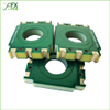
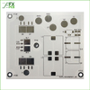
Description: or heat dissipation, this PCB is a very good option. Let’s investigate Aluminum PCB in more detail. What are its benefits over conventional PCBs, as well as its primary uses? Before investigating aluminum PCBs, it is important to understand what a PCB is. The term
- Thickness: 0.01968503937007874 to 0.1968503937007874 inches
- Materials: Aluminum Foil / Cladding, Copper Foil / Cladding
- Features: Specialty / Other


Find Suppliers by Category Top
Featured Products Top
-
 power, signal, and fiber optic pathways within a single hermetic assembly. These include high-voltage vacuum feedthroughs, PotCon® connector systems, PCB-integrated seals, and multi-port flange assemblies designed for dense, high-performance equipment architectures. Advanced low (read more)
Browse Feedthroughs Datasheets for Douglas Electrical Components -
Our Surface Preparation Solutions for both innerlayer and outerlayer cleaning address the challenges confronted by PCB fabricators, including the complex processing of increased layer counts, as well as the demands posed by harsh mechanical cleaning methods. Innerlayer (read more)
Browse Cleaning Agents and Surface Treatments Datasheets for MacDermid Alpha Electronics Solutions -
-toxic cleaning agents for PCBs and semiconductor equipment. They remove oil, grease and particles without damaging components and are compatible with solvent recovery systems for sustainability. AFLAS® fluoroelastomers: These materials are designed for (read more)
Browse Industrial Coatings Datasheets for AGC Chemicals Americas, Inc. -
ensure optimal performance. Fluoropolymer Coatings on Circuit Boards As cellular network technology advances, printed circuit boards face higher performance and quality demands. AGC’s Fluon+™ EA-2000 functionalized perfluoro resin coats and protects PCBs by (read more)
Browse Polymers and Plastic Resins Datasheets for AGC Chemicals Americas, Inc.
Conduct Research Top
-
Acid Copper Electroplating Process with Excellent V Pit Resistance for Flash Etching
to the electronics industry, but are common processes in IC substrate and PCB fabrication. They help maximize the PCB real estate usage by allowing fabricators and designers to build up multilayer devices. Figure 1 shows examples of multilayer designs that require multiple metallization and etching steps
-
Laser Ablation: The Alternative to Chemical Etching and Solder Dams
Laser ablation is a process that product manufacturers may wish to consider when looking to remove unwanted materials from a part's surface or when they wish to control solder flow on a PCB - typically so excess solder does not travel where it's not supposed to and cause electrical shorting
-
PCB Fabrication Basics: How Traces Are Made
, there is increased opportunity for lateral material removal. After some time in the etching tanks, liquid etchant removes copper both perpendicular and parallel to the board surface.
-
Measuring the Volume of Integrated Circuit Chipping After the Dicing Process Using a Digital Microscope
are oxidized, and an intricate, microscopic circuit pattern is added to them through photoresist coatings, pattern printing, etching, impurity diffusion, and planarization. Once the circuits are formed, the circular wafer is cut into small squares with a metal blade or laser during the dicing
More Information Top
 Indicates content that may require registration and/or purchase.

-
Powerstax Powers Green Manufacturing and Water Purification Systems
… to wash car bodies during their manufacture, purifying water used in the dairy and food industries by extracting blood etc, removing metals out of mountain streams for the brewing industry and recovery of cupric & ammonia cal copper in PCB etching equipment .
-
Design of linearly fed shaped-beam pattern microstrip antenna array
Because of the miniature of the array, ordinary PCB etching equipment is not accurate enough to make the array.
-
Used Manufacturing & Processing Machinery Manufacturers, Used Manufacturing & Processing Machinery Product Catalogs Directory
Related Searches : used, noristu, digital minilab, press machine, spiral pipe mill, roll forming machine, film processor, etching machine, pcb equipment More...
-
A Novel Nitric Acid Etchant and Its Application in Manufacturing Fine Lines for PCBs
It contains a copper foil 18 m in thickness, and the equip- ment of production line for spray etching was purchased from Huge Dragon PCB equipment Co., Ltd. (Guangzhou, China).
-
CR4 - Thread: Gold Off PCB
The traces that are etched onto the circuit board (pcb) are not gold (none that I have ever seen, even really high end equipment ); the traces on a pcb are always etched (acid bath burns in) to become copper.
-
Anglia Designs opens technology centre and EMC test chamber
It has a fully equipped laboratory, a wet room that includes a PCB etching , drilling and environmental chamber, and a custom-built EMC test chamber designed to help Anglia customers achieve pre-compliance for their electronic products through accurate measurement of conducted …
-
Electro-optical printed circuit board (EOPCB)
But because there is no need for such an anisotropic etching step in conventional PCB manufacturing, cost-intensive additional equipment , like the N E system,would have to be added to the process.
-
Glob-top reliability characterisation: evaluation and analysis methods
Successful and selective removal of epoxy on PCB assemblies has been demonstrated on 'jet- etch ' type decapsulation equipment using nitric and sulphuric acid mixes.
-
Fast and easy single step module assembly for back-contacted c-Si solar cells with conductive adhesives
Processing steps include printing of etch resist, etching, and stripping of etch resist, which can be done with standard equipment used for flexible PCB manufacturing.
-
Federal Register > Wednesday, February 11, 1998 > [63 FR 6956] Advice Concerning the Proposed Expansion of the Information Technology Agreement
Apparatus for wet etching , developing, stripping or cleaning PCB /PWBs and their connectors including cleaning equipment , horizontal/vertical wet processing equipment, finger plating equipment.