
Products & Services
See also: Categories | Featured Products | Technical Articles | More Information-
Supplier: Texas Instruments
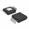
Description: RF-HDT-AJLE Tag-it(TM) HF-I Standard Transponder Chip (Wafer, bumped, inked, grind, sawn on tape)
- Operating Frequency: 13.56 MHz
- TJ: -25 to 70 C
- Technology: Wi-Fi / WiMAX / Wi-Mesh
-
Supplier: Texas Instruments
Description: RF-HDT-AJLS Tag-it(TM) HF-I Pro Transponder Chip (Wafer, bumped, inked, grind, sawn on tape)
- Operating Frequency: 13.56 MHz
- TJ: -25 to 70 C
- Technology: Wi-Fi / WiMAX / Wi-Mesh
-
Supplier: Swiss Jewel Company
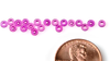
Description: Aperture Wafers are precision controlled orifices where the ID Length is controlled very tightly. Typical Applications: Hematology Instrumentation, Ink Jet Printing, Flow Control.
- Orifice Diameter: 0.0016 to 0.0395 inch
- Media: Chemical, Hydraulic Fluids, Ink, Other Gas, Pneumatic Air
- Applications: Flow Measurement, Ink Jet Printing
- Features: Other
-
-
Supplier: Henkel Corporation - Industrial
Description: LOCTITE CT 5030 E&C, Epoxy, Conductive Ink LOCTITE CT 5030 E&C is a conductive ink designed to provide thin coating used in shielding and grounding applications. It is electrically conductive, resistant to abrasion, crease resistant and heat resistant. It is also used in creating
- Substrate: Metal
- Industry: OEM / Industrial
- Form: Transfer Tape
-
Supplier: Henkel Corporation - Electronics
Description: (Known as HYSOL ECCOCOAT CT5030 Catalyst B97 conductive ink ) LOCTITE CT 5030 E&C is a conductive ink designed to provide thin coating used in shielding and grounding applications. It is electrically conductive, resistant to abrasion, crease resistant and heat resistant. It is also
-
Supplier: Acme Chip Technology Co., Limited
Description: WAFER UNSAWN, 725U, WITH INKING
- Features: Other
- Device Type: Sensor Interface
-
Supplier: Quarktwin Technology Ltd.
Description: WAFER UNSAWN, 304U, WITH INKING
- TJ: -40 to 85 C
- Features: Other, RoHS Compliant
- Device Type: Storage Interface
-
Supplier: Chonghong Industries(Microwork)Ltd.
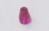
Description: Sapphire & Ruby Nozzles are used where a longer Inner Diameter to Length ratio is desired. Sapphire nozzles & Ruby offer longer life than using metal and we can hold tighter tolerances due to sapphires & Ruby acceptance of higher surface finish. Typical Applications: Gas & Air Flow, Wafer Jet
- Media: Air / Gases, Coatings / Inks
- Application: Cleaning / Blowoff, Cutting / Machining
- Features: Other
-
Supplier: Swiss Jewel Company
Description: Sapphire Nozzles are used where a longer Inner Diameter to Length ratio is desired. Using sapphire nozzles will provide longer life than using metal and we can hold tighter tolerances due to sapphires acceptance of higher surface finish. Typical Sapphire Nozzle Applications: Gas & Air Flow,
- Orifice Size: 9.5 to 30 mil
- Media: Air / Gases, Coatings / Inks, Water
- Application: Cleaning / Blowoff, Cutting / Machining
- Form: In-line
-
Supplier: Videojet Technologies, Inc.
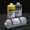
Description: Videojet inks and fluids are designed, tested and manufactured together, to function together at optimum performance levels, no matter what your application or production environment.
- Industry: Electronics, Food and Beverage, Medical / Healthcare, Military Specification, OEM / Industrial, Semiconductor / Wafer
- Features: Heat Resistant / High Temperature
- Type: Ink, Marking Material
-
Supplier: Saint-Gobain Surface Conditioning Group
Description: of your particular application, or a custom-engineered product can be made, if required. Applications Media filler: Video tapes, audio tapes, data storage devices, ink jet media Polishing abrasive Thermal management additive Frictional additive Wear resistance additive Metal matrix Structural
- Compound / Abrasive Type: Aluminum Oxide
- Grading System: Micron Graded
- Type: Polishing
- Form: Powder
-
Supplier: Saint-Gobain Surface Conditioning Group
Description: application, or a custom-engineered product can be made if required. Applications: Media Filler: Video and audio tapes, data storage devices, ink jet media Polishing abrasive Thermal management additive Wear resistance additive Metal matrix Structural ceramics
- Compound / Abrasive Type: Aluminum Oxide
- Grading System: Micron Graded
- Type: Polishing
- Form: Powder
-
Supplier: CoorsTek
Description: Ink Manifolds Ceramic Bushings Read-Write Head Manufacturing Tooling Coil Insulator Housings
- Material Type: Alumina / Aluminum Oxide
- Applications: Electrical / HV Parts, Electronics / RF-Microwave
- Shape / Form: Fabricated / Custom Shape, Wafer / Substrate
-
Supplier: Matexcel
Description: material in biological and electronic applications and quantum engineering. Source: Synthesis Storage: Store at room temperature. Application: For PET products, inks, rubbers, glues, paints, For wafers & PCB cleaning agents Purity: >99% Concentration: 0.07 CAS Number: 7782-40-3 Size:
-
Supplier: Abrisa Technologies
Description: Substrate Materials SCHOTT BOROFLOAT® 33 – Low CTE, High T% SCHOTT D 263® T eco Ultra-Thin Low Iron Soda Lime – Economical Float Material Low & Non-Alkaline, Corning® Eagle XG® Corning® Gorilla®, AGC Dragontrail®, SCHOTT AS 87 Customer Furnished Materials & Wafers Our ITO, IMITO, and IMO
- Features: Electric, Other







Find Suppliers by Category Top
Featured Products Top
-
 Element Solutions Inc (ESI) announced the completion of its acquisition of the Micromax conductive pastes and inks business, effective February 2, 2026. Micromax will operate within MacDermid Alpha Electronics Solutions, part of ESI’s Electronics segment. The (read more)
Browse Electrical and Electronic Resins Datasheets for MacDermid Alpha Electronics Solutions
Conduct Research Top
-
EETimes.com | Electronics Industry News for EEs & Engineering Managers
11 to 17 ATE consortium signs on TEL, strikes alliance in China 3M sets up service to address CVD, CMP issues : Sumco to become profitable Taiwan index climbs amid surge in chip-outsourcing services TSMC may hike capex to meet huge wafer demand Xerox devises 'semiconductive ink' for flexible TVs
More Information Top
 Indicates content that may require registration and/or purchase.

-
Optical inspection of MOEMS devices using a configurable and suitable for production image processing system
Results are stored in wafer maps which can be directly used for wafer inking .
-
Semicon West 2013 to Feature Amicra’s Latest Die and Flip Chip Bonders
With its broad product line of semi-automatic (SIS) and fully automatic wafer ink (AIS) systems, Amicra is currently setting industry standards at a dot size down to 125 µm, and for the inking of diced or undiced wafers.
-
Optimizing the Cost of Test at Intel Using per Device Data
Historically, wafer lots were sorted and a pass/fail decision was documented on each unit via an "ink dot" (hence the term wafer inking ).
-
"Chevron"-type piezoelectric inkjet actuator
Through an opening in the cover wafer ink is fed into the channels.
-
http://dspace.mit.edu/bitstream/handle/1721.1/38050/33213898-MIT.pdf?sequence=2
These inked wafers are then shipped from the fabrication site to the assembly site.
-
A framework and architecture for rapid software development: a success story
Savings are incurred by not having to ink wafers to mark faulty dice before sending them to assembly.
-
Chemical Aspects of Water Quality and Health
&' inking Wafer .