 | PrefaceThis book grew out of a series of courses that I developed and taught over many years in the areas of lasers, optoelectronics, and photonics. Although these courses have been taught in the physics department, I have made a conscious effort to keep them accessible to nonphysics majors, especially sophomores and juniors from engineering or the other sciences. These students are typically looking for a survey course to introduce them to the basic elements of photonics and lasers, often to fulfill a science "distribution requirement." It has always been difficult to find an appropriate textbook for such a course because the existing books in these areas are aimed at either too high a level or too low a level, or they cover only a portion of the topics that are needed. In teaching these classes, I came to rely mostly on my lecture notes as the reading material for the course. This need for a truly introductory level book, covering a wide range of topics in photonics and lasers, was my motivation for writing this book. |
In deciding what material to include, and how to present it, I have kept two distinct audiences in mind. One is the college undergraduate described above, and the other is the working professional who wants to "come up to speed" in the photonics area by learning the fundamentals in an accessible format. Both of these audiences, I believe, can benefit from the level of treatment given here. The reader's physics background is expected to include the usual freshman-level sequence of courses in mechanics, electricity and magnetism, waves, and modern physics. Knowledge of differential and integral calculus is assumed, including simple ordinary differential equations, but no knowledge of partial differential equations is needed. Although I do present and discuss certain solutions of Maxwell's equations that are relevant for photonics (such as the Gaussian beam), I do not derive these solutions here. Similarly, I discuss topics relating to quantum mechanics at the de Broglie wave and "particle in a box" levels, without ever writing down the Schrödinger equation. Readers with a more advanced physics background will better appreciate some of the points that are made, but the bulk of the material should be understandable by those with only a modest physics background. My goal throughout has been to make sure that the mathematics does not get in the way of the physical concepts. I've tried whenever possible to give physical arguments that lead to an intuitive understanding, while including sufficient mathematical detail to make that understanding quantitative as well. This is a tough balancing act, and necessarily results in trading off rigor versus accessibility. I have deliberately avoided the temptation to be "comprehensive," choosing instead to limit the discussion when appropriate to certain limiting cases that are mathematically simple. This not only makes the discussion easier to follow for the beginning student, but also brings out the fundamental concepts more clearly. To further aid the student who is just learning to think symbolically, I have written some equations in words as well as symbols. The topical coverage in this book is somewhat unusual, in that it treats two subjects photonics and lasers that are usually found in separate books. One reason they are included together here is that there is a natural synergy between them. On the one hand, understanding the operating principle of certain lasers requires knowledge of photonics concepts such as waveguiding, while on the other hand, understanding the principles of optical communications (an important photonics system) requires some knowledge of lasers. An additional benefit to treating them together is a consistency of notation, which is very helpful to the beginning student. An annotated list of symbols is provided at the end of the book. Because of the combined coverage of photonics and lasers, it is probably unrealistic to try to cover the entire book in a one-semester course. If a course emphasizes photonics, a suggested list of chapters to cover would be 1-7, 10-15, and 24. Chapters 8 and 9 are additional options, should time permit. A course emphasizing lasers might cover Chapters 2, 10-11, and 15-23, with Chapter 9 optional if time permits. Different combinations of chapters or parts of chapters can certainly be used, depending on the emphasis of the particular course. I would like to thank the many students who have taken my classes over the years, for their questions and comments. You have been my inspiration, and your struggles with the course material have helped me to sharpen my presentations, ultimately making this a better book. Thanks are also due to the reviewers commissioned by Cambridge University Press and Wiley who took the time to make helpful comments on the manuscript. And, finally, thanks to my wife Julie and daughters Claire and Grace, for putting up with the many long hours that took me away from family life. This project could not have been completed without your patience and understanding. R. S. Quimby Worcester Polytechnic Institute | |
 TABLE OF CONTENTS
 Chapter 14.4 - Types of Photodiodes
14-4. TYPES OF PHOTODIODES
|

 . In this regime, Eq. (13-15) gives
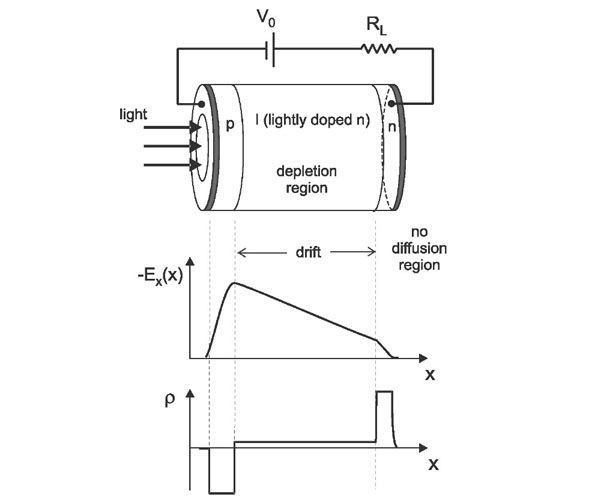


 2 × 10⁶ V/m, so