Breakdown Phenomena in Semiconductors and Semiconductor Devices
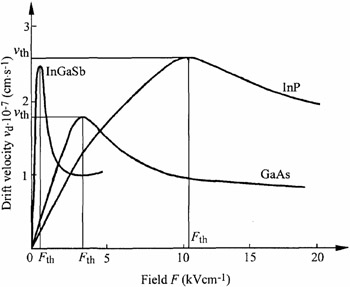
Let us consider for the sake of definiteness a n + - n - n + structure. If the bias V 0 is applied to a dielectric bar of length L, the field F across the sample will simply be equal to V 0/ L. For a semiconductor sample, however, the situation can be more complicated. To explain the point, let us start from the most illustrative case, that in which the carrier drift velocity in the semiconductor decreases with field growth at high fields (negative differential conductivity; NDC). As mentioned in Chapter 3, such a situation occurs in GaAs, for example. In fact there are many semiconductors, such as InP, InSb, InAs [2], many A 3B 5 ternary and quaternary compounds [18], GaN, and (presumably) SiC [19], in which the electron drift velocity in a certain range of electric fields decreases with an increase in the electric field (Figure 4.1).
The current density
| (4.1) | |
does not depend on the coordinate x. (Here we...