Compound Semiconductor Bulk Materials and Characterizations

InAs is a narrow bandgap semiconductor and is useful in very high speed electronic devices. It is also used as a substrate for infrared detectors and Hall devices and used assource material for multinary compound epitaxial growth.1
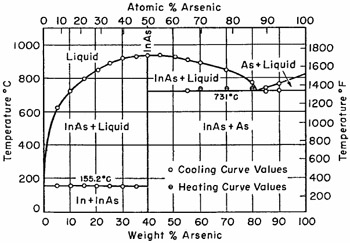
The physical properties of InAs2 , 3 are summarized in Table 11.1. The melting point of InAs is 943 C, rather low compared with other III-V materials. The bandgap is as low as 0.356 eV and electron mobility is as high as 33,000 cm 2/V.sec so that it can be expected to be a good material for long wavelength photodetectors and high speed electronic devices. The phase diagram of InAs is as shown in Fig. 11.1.4 , 5 The decomposition pressure of InAs is as low as 0.33 atm. at the melting point.6 The thermoelectrical properties of InAs have been evaluated and found to be 210 310 ?V/K.7
| Crystal Structure | zincblende |
| Lattice Constant | 6.058 |
| Density | 5.667 g/ cm 3 |
| Melting Point | 943 C |
| Linear Expansion Coefficient | 5.19 10 -6/ deg |
| Thermal Conductivity | 0.26 W/cm K |
| Dielectric Constant | 14.55 |
| Refractive index | 3.52 |
| Bandgap at Room Temperature | 0.356 eV |
| Intrinsic Carrier Concentration | 1.25 10 15/ cm 3 |
| Electron Mobility | 33,000 cm 2/V sec |
| Hole Mobility | 460 cm 2/V sec |
| Conductivity | 0.2 ? cm |
InAs is industrially grown by the Liquid Encapsulated...