Compound Semiconductor Bulk Materials and Characterizations
Part 3: II-VI Materials

CHAPTER LIST

Chapter 13: CdS
Chapter 14: CdSe
Chapter 15: CdTe
Chapter 16: Zns
Chapter 17: ZnSe
Chapter 18: ZnTe

13.1 INTRODUCTION

After the photovoltaic effect was first observed by Reynolds et al.,1 much interest was focused on CdS. CdS is a material which is of importance in phosphors and photoconductors. Since the bandgap of CdS is 2.3 8 eV and of direct transition type, it is a candidate for green light photoelectric conversion devices. CdS is also promising for lasers so that the growth of large single crystals have been attempted.

13.2 PHYSICAL PROPERTIES

Typical physical properties are shown in Table 13.1. 2 6 Precise melting point and vapor pressures were determined by Addamiano et al.7 , 8

Table 13.1: Physical Properties of CdS

Crystal Structure

wurtzite

Lattice Constant

a=4.1368

c=6.7163

Density

4.82 g/cm 3

Melting Point

1475 C

Linear Expansion Coefficient

5.0 6.5 10 -6/deg( ?c)

2.5 4.0 10 -6/deg(//c)

Thermal Conductivity

0.3 W/cm K

Dielectric Constant

10.33 (//), 9.35 ( ?)

Refractive index

2.674

Bandgap at Room Temperature

2.38 eV

Optical Transition Type

direct

Intrinsic Carrier Concentration

16.7 10 15/cm 3(1173K)

Electron Mobility at R.T.

350 cm 2/V sec

Hole Mobility at R.T.

15 cm 2/V sec

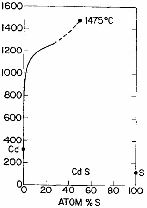
The phase diagram of CdS was reported by Woodbury9 as shown in Fig. 13.1. The lattice parameter of CdS xSe 1-x has been measured by Al-Bassam et al.10


Figure 13.1: Phase diagram of CdS (reprinted from Ref. 9...

UNLIMITED FREE
ACCESS
TO THE WORLD'S BEST IDEAS

SUBMIT
Already a GlobalSpec user? Log in.

This is embarrasing...

An error occurred while processing the form. Please try again in a few minutes.

Customize Your GlobalSpec Experience

Category: Inorganic Chemicals and Compounds
Finish!
Privacy Policy

This is embarrasing...

An error occurred while processing the form. Please try again in a few minutes.