Nanoelectronics and Photonics: From Atoms to Materials, Devices, and Architectures
Color Insert


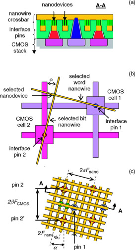
Fig. 4.4: The generic CMOL circuit: (a) a schematic side view, (b) a schematic top view showing the idea of addressing a particular nanodevice via a pair of CMOS cells and interface pins, and (c) a zoom-in top view on the circuit near several adjacent interface pins. On panel (b), only the activated CMOS lines and nanowires are shown, while panel (c) shows only two devices. (In reality, similar nanodevices are formed at all nanowire crosspoints.) Also disguised on panel (c) are CMOS cells and wiring

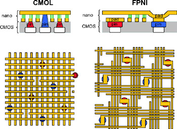
Fig. 4.7: Comparison of CMOL and HP's FPNI circuits (adapted from Ref. [42])

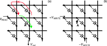
Fig. 4.9: Equivalent circuits of the crossbar memory array showing (a) read and (b) write operations for one of the cells (marked A). On panel (a), green arrow shows the useful readout current, while red arrow shows the parasitic current to the wrong output wire, which is prevented by the nonlinearity of the I V curve of device A (if the output voltage is not too high, V out < V t)

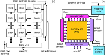
Fig. 4.10: CMOL memory structure: (a) global and (b) block architectures

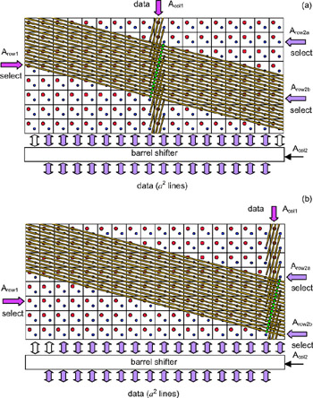
Fig. 4.11: CMOL block architecture: Addressing of an interior column of nanowire segments (for a = 4). The figure shows only one (selected) column of the segments, the crosspoint nanodevices connected to one (selected) segment, and continuous top-level nanowires connected to these nanodevices. (In reality, the nanowires of both layers fill...

UNLIMITED FREE
ACCESS
TO THE WORLD'S BEST IDEAS

SUBMIT
Already a GlobalSpec user? Log in.

This is embarrasing...

An error occurred while processing the form. Please try again in a few minutes.

Customize Your GlobalSpec Experience

Category: Nanomaterials
Finish!
Privacy Policy

This is embarrasing...

An error occurred while processing the form. Please try again in a few minutes.