General Amplifier Concepts
An amplifier can be represented as a two-port device. The two ports are called input and output. Each port has two terminals, and in general one of the terminals is ground. When a voltage (vi) is applied at the input terminals, an output voltage (vo) is generated at the output terminal. The voltage vi is normally generated by a signal generator or source that has an internal resistance Rs. Normally, the output voltage of the amplifier is applied to a load which is represented by a resistor RL. The general characteristics of any amplifier are related to the following three parameters:
The no–load voltage Gain: This parameter is defined as
|  | (14.1)
|
The Input Impedance: Zi, defined by
|  | (14.2)
|
and
The Output Impedance: Zo, defined by
|  | (14.3)
|
The no–load voltage gain, Avnl, as its name implies, is calculated by determining or measuring the input and output voltages when there is no load connected to the output of the amplifier. Avnl is the ratio of the output voltage to the input voltage. This gain is the highest gain you can achieve. Generally, this gain is given by the manufacturer when you buy the amplifier.
The input and output impedances are the Thèvenin impedances calculated at the amplifier input and output respectively. In order to determine them you must apply the general methods used to calculate Thèvenin equivalents.
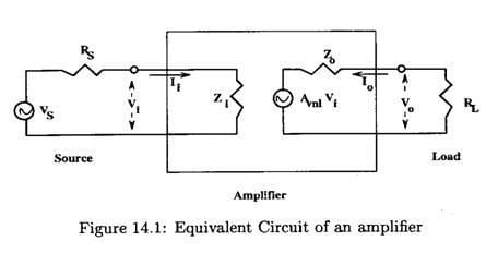
Once these parameters are known the amplifier can be represented by the equivalent circuit of Figure 14.1.
Notice that in this representation we have included in the diagram the source (together with its internal resistance, Rs) and the load which is represented by the Thèvenin resistance RL. The amplifier is the box shown in the figure. The amplifier, then, is represented by the input impedance, Zi from the input point of view and by a source (AvnlVi) and an impedance (Zo) from the output point of view.
The Voltage Gain
The complete system, as you can see, can be analyzed by solving two very simple loops: each one has one source and two impedances. The voltage gain when there is a load and a source is different from the voltage gain when there is no load (Avnl). To determine the voltage gain – and in the same way, the current gain – for a general amplifier, we proceed as follows: the output voltage, from the output loop, is given by the equation
|  | (14.4)
|
Now, to determine the voltage gain divide the right-hand side and the left-hand side of Eq. 14.4 by vi, in order to cancel vi from the RHS of the equation. This will leave the LHS to be  , which is precisely the voltage gain of the amplifier when there is a load connected to it. This process will give you the formula for the voltage gain. This important formula is
| 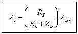 | (14.5)
|
From the above equation we can see that the gain (with load) of the amplifier is dependent on the value of the load. For different loads we have different gains. This feature is known as the loading effect. To illustrate this idea let’s find the voltage gain for the following two extreme cases.
Open Loop If the load is an open loop this means that there is no load connected to the amplifier1. To determine the gain let’s write Eq. 14.5 in a different format. Divide numerator and denominator by RLand get the alternate equation
Now, when RL = ∞ the denominator of the above equation becomes 1 and the gain is
|  | = |  | (14.7)
|
This is, as you may know by now, what is expected. When the load is equal to ∞ there is no load and thus the gain should be equal to the voltage gain without load.
Short Circuit If the load is a short circuit (RL = 0) the gain of the amplifier becomes zero (0), as you can see from Eq. 14.5. This is also expected because if the output is a short circuit the voltage must be zero, so the gain will be zero.
If the load is between those two extreme cases (i.e., when RL is of some finite value) the voltage gain will be between the voltage gain values of Av = 0 and Av = Avnl2. In other words, the maximum voltage gain of any amplifier is Avnl. This is a very important fact to remember.
1 Remember that an open loop is represented by an infinite resistance.
2 This is precisely the voltage gain given by Eq. 14.5,
The Current Gain
The current gain is found as follows: the output current is given by
and
|  | (14.9)
|
Thus, Eq 14.8 becomes
|  | (14.10)
|
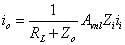
Dividing the RHS and the LHS of the above equation by ii and rearranging, we get the current gain
|  | (14.11)
|
To obtain a simpler formula for the current gain, we notice that by dividing numerator and denominator of Eq. 14.11 by RLwe can write the current gain in terms of the voltage gain3 as follows:
|  | (14.12)
|
3 Many times it is easier to determine the voltage gain rather than the current gain directly.The Power Gain
The power gain of an amplifier can be found by multiplying the voltage gain by the current gain, or
|  | (14.13)
|
The Overall Voltage Gain
Eq. 14.5 is the formula for the voltage gain of the amplifier when we consider only the input voltage (vi) at the input terminals of the amplifier and the output voltage (vo) at the output terminals. Therefore, this equation is the ratio between the output and input voltages, or in an equation form
| 
| (14.14)
|
|
In order to apply this equation we must first calculate the input voltage at the input terminals. As you know this voltage is a function of the source voltage. From Fig. 14.1 we see that this voltage is given by4
|  | (14.15)
|
where Rs and vs are the source resistance and source voltage respectively.
Many times we will need to determine the overall voltage gain of an amplifier. This, by definition, is the ratio of the output voltage, vo, to the source voltage, vs. To determine this quantity, first let’s find a generic formula for this gain. This ratio can be expressed in general by the following relations
|  | (14.16)
|
|  | (14.17)
|
We notice that in the above equation the first ratio is the voltage gain given by Eq. 14.5 and the second fraction is the fraction of the source voltage that will be applied at the input terminals of the amplifier. This fraction can be found by using Eq. 14.15. By dividing the RHS and LHS of this equation by vs we get the desired expression
|  | (14.18)
|
Now we can rewrite Eq. 14.16 using Eq. 14.18 and Eq. 14.5. The resulting overall voltage gain is given by
| | |
(14.19) | |
|
|  | (14.20)
|
Notice that the overall voltage gain given by Eq. 14.20 includes the load resistance and the source resistance. If there is no load connected to the amplifier, then the second fraction in Eq. 14.20 becomes one (1). If, on the other hand, there is no source resistance the first fraction becomes one (1) and the overall voltage gain ( ) is equal to the normal voltage gain ().
4 Apply the voltage divider rule to the input impedance, Zi.Common-Emitter Amplifier
Now that you know the general ideas of amplifiers, let’s look at the common-emitter amplifier. This amplifier is built with only one transistor. The body of the amplifier is the common-emitter DC bias circuit of Equipment 10. Figure 14.3 shows a complete common-emitter amplifier with a source, source resistance and load.
To determine these AC parameters of the CE amplifier it is necessary to represent the transistor with a simple model. The most popular model for the BJT transistor is the so-called re-model.
As you should know, the re-model represents the transistor by means of the following circuit

To use this model in our calculations it is necessary to calculate the AC emitter resistor, re. The following section outlines the procedure.
How to determine re
To determine the value of re follow these steps:
□ Solve for the DC parameters of the amplifier. (See Experiment 10)
□Calculate re with the following formula:
|  | (14.21)
|
where IE is the DC emitter current5 The common-emitter amplifier of Fig. 14.3 is the circuit we will follow to determine the AC parameters. 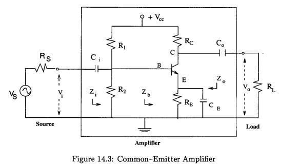
Several cases will be considered. With CE No Load (RL = ∞): |
This is the case of the no-load circuit. For this case, the amplifier parameters are as follows:
|  | (14.23)
|
Without CE, No load (RL = ∞): |
If RE is much larger than re (which is normally the case), then the open-loop voltage gain can be approximated to
5 Review section 10.5.1.1 on page 115.
Effect of load on the voltage gain: If there is an actual load, RL, the voltage gain for each case will be given by: for the case with the bypass capacitor, CE, and or when there is no bypass capacitor, CE. Note that if you know the load of the system you can use Eq. 14.5 to find the voltage gain with load. This should produce equations 14.31, 14.32 and 14.33. The current gain for any of the cases presented above is given in terms of the voltage gain, by the following formula: when there is no actual load, and for the case when a load, RL, exists in the system. The Overall Voltage Gain:
The voltage gain calculated from the above formulas is for the voltage gain without including the effect of the source resistance, Rs. This is the voltage gain defined according to Av = vo/vi, where the input voltage, vi, is the input voltage to the amplifier. To include the effect of the source resistance, Rs, as you know, we have to re-define the voltage gain as follows: This is called the overall voltage gain, and it is calculated by including the attenuation produced by the source resistance. For any CE amplifier, the overall voltage gain is given by where Av is the voltage gain given by anyone of the Equations 14.25, 14.29, 14.30, 14.31, 14.32 and 14.33. | To determine the output voltage, vo : |
To find the AC output voltage of any amplifier, proceed as follows: □ Find the voltage gain for the appropriate case. This may be AV or depending on what is given in the problem. □ Determine vo by one of these two formulas:
© 2026 GlobalSpec, Inc.
|
 This book is designed for students who are taking their first course in analog electronics in either a two-year or four-year program. The prerequisites are a DC-AC course; a basic knowledge of algebra, including the ability to solve simultaneous linear equations; and a strong knowledge of trigonometry. The main topics in this book provide an introduction to the most important semiconductor devices: how they are built, how they operate, and how they are used in larger electronic modules.