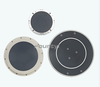
High-Precision Ceramic Wafer Chucks
Featured Product from Fountyl Technologies Pte. Ltd.

High-purity alumina and aluminum nitride ceramic chucks, including porous ceramic chucks and electrostatic chucks (E-Chucks), provide high-precision positioning, uniform holding force, excellent thermal management, and outstanding plasma corrosion resistance. They are widely used in critical semiconductor manufacturing processes such as photolithography, etching, thin-film deposition, and chemical mechanical polishing (CMP).
Non-destructive Uniform Clamping:
Uniform vacuum adsorption or electrostatic force minimizes mechanical stress and protects fragile substrates and precision workpieces from damage.
Nanometer-level Flatness:
Sub-micron surface accuracy meets the stringent requirements of advanced semiconductor manufacturing for precise positioning and stable support.
Superior Thermal Management:
Accurate temperature control and rapid heat dissipation improve process stability, consistency, and production yield.
Ultra-high Cleanliness:
Low outgassing characteristics and excellent plasma corrosion resistance make these chucks ideal for ultra-clean vacuum processing environments.
Applications
Wafer Manufacturing:
Wafer stages for photolithography systems, etching chucks, electrostatic chucks for ion implantation equipment, and thin-film deposition systems.
Inspection and Packaging:
Wafer probing stations, wafer inspection equipment, and wafer-level packaging (WLP) carriers.
Optics and Display Panels:
Vacuum chucks for OLED flexible display inspection, handling platforms for LCD glass substrates, and precision positioning systems for optical components.