Silicon Carbide Wafer Pins and Chucks
Featured Product from Fountyl Technologies Pte. Ltd.
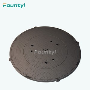
Silicon carbide wafer pins and chucks are used in plasma etch chambers, CVD systems, and ion implantation equipment for wafer support, lifting, and clamping during processing. The material must withstand aggressive plasma chemistry while maintaining dimensional stability and minimizing particle generation.
Material Grade
Fountyl uses high-purity sintered silicon carbide (SiC) with the following specifications:
- Purity -- >= 99%
- Density -- >= 3.10 g/cm3 (theoretical density > 98%)
- Flexural strength -- >= 450 MPa (room temperature)
- Vickers hardness -- >= 2500 HV
- Thermal conductivity -- >= 150 W/m.K (room temperature)
- Maximum service temperature -- 1600 C (inert atmosphere)
- Surface resistivity -- 10^4-10^6 ohm/sq (semi-insulating grade available on request)
Product Configurations
- Wafer pins -- Diameter 3-10mm, length 20-200mm. Tip options: flat, radiused, or grooved. Used as lift pins in etch and deposition chambers.
- Pin holders / guides -- Precision-ground bore tolerance H7. Matching pin-to-guide clearance 0.01-0.03mm.
- Wafer chucks -- Diameter 150mm, 200mm, and 300mm formats. Flat or grooved surface. Custom OD and vacuum hole patterns available.
- Ring chucks -- Annular design for edge-grip wafer clamping. ID matched to wafer edge exclusion zone.
Surface and Dimensional Tolerances
- As-sintered surface -- Ra <= 3.2um, for general chamber components
- Ground surface -- Ra <= 0.8um, for pin contact tips and chuck seating surfaces
- Lapped surface -- Ra <= 0.2um, for applications requiring minimal friction or particle trapping
- Dimensional tolerance -- +/-0.05mm on pin diameter, +/-0.1mm on chuck OD. Higher precision available on request.
Typical Chamber Applications
- Plasma etch chambers -- SiC pins and chucks resist fluorine-based and chlorine-based plasma. No coating required. Minimal erosion rate extends component lifetime between PM cycles.
- CVD and PECVD -- Thermal stability at deposition temperatures up to 800 C. No outgassing, no metal contamination.
- Ion implantation -- Semi-insulating SiC grade dissipates charge buildup during ion beam exposure, reducing wafer charging damage.
Quality and Packaging
Each part is visually inspected and dimensionally checked. Surface quality verified under 10x magnification. Parts are cleaned in DI water ultrasonic bath and packaged in cleanroom-compatible sealed bags. Custom pin tip geometries, chuck groove layouts, and vacuum port configurations can be engineered to match existing chamber designs.
Fountyl Technologies Pte. Ltd. supplies SiC wafer pins and chucks to semiconductor equipment OEMs and fab maintenance teams. Production includes powder processing, sintering, precision grinding, and final cleaning in-house.