
-
Supplier: Accuris
Description: Fraises 3 tailles, \xe0 al\xe9sage lisse, \xe0 entra\xeenement par clavette - S\xe9rie m\xe9trique
-
Supplier: Accuris
Description: Rondelles plates - S\xe9rie large - Partie 2: Grade C
-
Supplier: Accuris
Description: Fraises cylindriques 2 tailles, \xe0 al\xe9sage lisse, \xe0 entra\xeenement par tenons - S\xe9rie m\xe9trique
-
-
Description: UPD78F1235/78K0R/IE3 EVAL BRD
- Category: Development Board
-
Supplier: Accuris
Description: Conteneurs de la s\xe9rie 1 - Classification, dimensions et masses brutes maximales AMENDEMENT 2
-
Supplier: Gelest, Inc.
Description: Additional Properties Hydrolytic Sensitivity 7: reacts slowly with moisture/water Application Precursor of vinylsilazane preceramic polymers.1 Reacts with photoresists to give RIE resistance.2 Intermediate for polyborosilazanes.3 Reference 1. Toreki, W. et al. Ceram. Eng. Sci. Proc. 1990, 11,
- Boiling Point: 222.8 to 228.2 F
- Flash Point: 185 F
- Purity: 92 %
-
Supplier: Gelest, Inc.
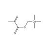
Description: Additional Properties Hydrolytic Sensitivity 4: no reaction with water under neutral conditions Application Comonomer with chloromethylstyrene for RIE resistant photoresist.1 Reference 1. Mixon, D. et al. J. Vac. Sci. Technol., B 1989, 7(6), 1723. Safety Packaging Under Nitrogen Store Cold
- Flash Point: 145.4 F
- Purity: 97 %
- Features: Metalloids (B, Si, Ge, etc.), Non-Metals (C, N, O, P, S)
- Type: OrganoMetallics
-
Supplier: Comdel, Inc.
Description: meet the performance demand in RF-driven plasma systems for semiconductor processing. Applications include etch, RIE, parallel plate, ICP, RF sputtering, CVD and PVD, as well as induction and dielectric heating processes in industrial systems, and solar photovoltaic applications. Features:
- Features: Adjustable Phase
- Form Factor: Rack/Card Mounted
-
Supplier: Plasma Etch, Inc.
Description: Built as an extension of our MK-II platform, it offers you the same repeatability, reliability and long life, as well as low maintenance costs. The Reactive Ion Etch (RIE) electrode offers the highest directional plasma effect. Etching with our roll to roll plasma etcher in the large all
- Materials Processed: Compound Semiconductors / GaAs, Metal, Tungsten / Refractory Metal
- Features: Gas Control Unit, Integral Process Controller, Other
- Vacuum / Pressure Range: Medium (< 1, >10-3 torr)
- Process: Plasma Etching / Cleaning
-
Supplier: Comdel, Inc.
Description: high reliability. Applications: The CX series is designed to meet the performance demand in RF-driven plasma systems for semiconductor processing. Applications include etch, RIE, parallel plate, ICP, RF sputtering, CVD and PVD, as well as induction and dielectric heating processes in
- AC Input Voltage: 190 to 230 volts
- Input Frequency: 50 to 60 Hz
- Output Frequency: 2 to 30 MHz
- Number of Outputs: 1 #
-
Supplier: Integrated Sensing Systems, Inc.
Description: No Description Provided
- Capabilities: 2D / Surface Micromachining, 3D / Bulk Micromachining, Dielectric / CVD Thin Film, Dry Etching (Plasma / RIE), Inspection / Testing, Metallization - Electroplating, Metallization - PVD Thin Film, Oxidation / Doping, Packaging / Backend Processing, Photolithography, Screen Printing, Wafer Bonding,
- Materials: Compound Semiconductor, Glass, Quartz, SOI, Silicon
- Services: Design / Engineering, Pilot / Scale-Up, Production, Prototyping, R & D / Development
- Features: Midwest US Only, North America, Specialty / Other, United States Only
-
Supplier: Universal Semiconductor, Inc.
Description: No Description Provided
- Capabilities: 2D / Surface Micromachining, 3D / Bulk Micromachining, Dielectric / CVD Thin Film, Dry Etching (Plasma / RIE), Inspection / Testing, LIGA, Metallization - Electroplating, Metallization - PVD Thin Film, Oxidation / Doping, Packaging / Backend Processing, Photolithography, Wafer Bonding, Wet /
- Materials: Ceramic, Compound Semiconductor, Glass, Metal / Nickel, Polymer / Organic, Quartz, SOI, Silicon
- Services: Design / Engineering, Pilot / Scale-Up, Production, Prototyping, R & D / Development
- Features: North America, Southwest US Only, Specialty / Other, United States Only
-
Supplier: Comdel, Inc.
Description: meet the performance demand in RF-driven plasma systems for semiconductor processing. Applications include etch, RIE, parallel plate, ICP, RF sputtering, CVD and PVD, as well as induction and dielectric heating processes in industrial systems, and solar photovoltaic applications. Features:
- Features: Adjustable Phase
- Form Factor: Rack/Card Mounted





Find Suppliers by Category Top
Featured Products Top
-
 semiconductor applications.” Outperforms in harsh plasma environments Perlast® Helios G7HA has been tested extensively in a series of plasma environments (RPS NF3, RIE NF3, CCP NH3, RIE SF6, RIE O2 and CCP (read more)
Browse O-rings Datasheets for Precision Polymer Engineering Ltd.
More Information Top
 Indicates content that may require registration and/or purchase.

-
Struktur‐ und magnetochemische Untersuchungen an KCuGaF 6
4994) und die aus den Oxiden gewonnenen Trifluoride eingesetzt: Al2O3 ( Rie - del de Haen, Nr.
-
AlN/GaN heterostructure TFTs with plasma enhanced atomic layer deposition of epitaxial AlN thin film
Device fabrication commenced with source/drain opening by Cl2/BCl3/Ar inductively-coupled- plasma reactive ion etching (ICP- RIE ) of Al2O3 and AlN followed by electron beam evaporation of a Ti/Au (20/150 nm) stack and lift-off.
-
http://repositories.lib.utexas.edu/bitstream/handle/2152/21457/XUE-DISSERTATION-2013.pdf?sequence=1
then defined by e-beam lithography and CF4 RIE using Al2O3 as the hard mask.
-
Characterization of Bragg gratings in Al2O3 waveguides fabricated by focused ion beam milling and laser interference lithography
Firstly, ridge waveguides varying between 1 mm and 10 mm in length, with an etch depth of 100 nm and a width of 3 μm were etched into the 1-μm-thick Al2O3 layers via RIE [2].
-
Feasibility Analysis of On-Wafer Microfocal Lens for Optical Coupling in Heat-Assisted Magnetic Recording Systems
R at about 3 nm [19], and RIE over alumina ( Al2O3 ) could contribute to nonuniformity h at around 15 nm [20].
-
A new single-pole-type head trimmed by focused ion beam at wafer level
The method is as follows; a) Grooves that have the track width is made by RIE on an Al2O3 layer; b) a magnetic film is deposited by electroplating on the grooves; and c) Chemical Mechanical Polishing (CMP) is used to remove the …
-
Selective etching of focused gallium ion beam implanted regions from silicon as a nanofabrication method
Liu et al have prepared RIE masks from ALD Al2O3 with a combination of FIB and wet etching, and stated that a 50 nm film is suited for blocking gallium ions for lithography purposes, i.e. FIB exposed oxide regions would be …
-
An advanced fabrication method of highly ordered ZnO nanowire arrays on silicon substrates by atomic layer deposition
The sample was etched by an RIE process and the Al2O3 was etched away.
-
A novel approach for nanoporous gas sensor fabrication using anodic aluminum oxidation and MEMS process
Finally, the aluminum oxide nanotubes acted as an dry-etch mask, as seen in figure 4(a), and RIE process etched through Al2O3 barrier layer to form nanoporous pores ranging 500~750 nm in diameter on silicon or silicon dioxide, as shown in …
-
Flexible and Semi‐Transparent Thermoelectric Energy Harvesters from Low Cost Bulk Silicon (100)
Subsequently, we performed a third lithography step to remove Al2O3 with reactive ion etching ( RIE ), leaving the contact areas exposed.