
Products & Services
See also: Categories | Featured Products | Technical Articles | More Information-
Supplier: Plansee SE
Description: impurities in the sputtering target are reproduced almost 1:1 in the sputtered functional layer and result in particle formation during the PVD process (arcing effect). We guarantee that our molybdenum targets have a purity of at least 99.97 %. The average purity of our
- Type: Sputtering Target
-
Supplier: Plansee SE
Description: and gaseous impurities in the sputtering target are reproduced almost 1:1 in the sputtered functional layer and result in particle formation during the PVD process (arcing effect). Sputtering targets made from high-purity materials are therefore required for the coating
- Type: Sputtering Target
-
Supplier: Plansee SE
Description: copper targets. They are present only in concentrations well below the critical threshold values. Maximum density. Our special production processes allow for our copper sputtering targets to have a density of nearly 100 %. As a result, your process benefits from a particularly
- Type: Sputtering Target
-
-
Supplier: Plansee SE
Description: layer and rapid sputtering due to high deposition rates. Outstanding purity. Metallic and gaseous impurities in the sputtering target are reproduced almost 1:1 in the sputtered functional layer and result in particle formation during the PVD process. We guarantee that our MoTa
- Type: Sputtering Target
-
Supplier: ASTM International
Description: 1.1 This specification covers pure titanium sputtering targets used as a raw material in fabricating semiconductor electronic devices. 1.2 This standard sets purity grade levels, physical attributes, analytical methods, and packaging.
-
Supplier: ASTM International
Description: This specification covers high purity titanium sputtering targets for use as raw material in the fabrication of semiconductor electronic thin films. Material covered by this specification comprises Grades 4N, 4N5, and 5N titanium sputtering targets, the grades of
-
Supplier: ASTM International
Description: This guide covers sputtering targets used as thin film source material in fabricating semiconductor electronic devices. It should be used to develop target specifications for specific materials. This standard sets purity grade levels, analytical methods and impurity
-
Supplier: Deposition Sciences, Inc.
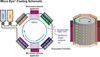
Description: MicroDyn sputtering process is that more than one sputtering target can be active at once. Co-sputtering two materials (a high index and low index) simultaneously allows the creation of a mixed layer with a controllable intermediate index. This extra degree of freedom
- Functions & Features: Abrasion Resistant, Antireflective, Chemical Resistant, Dielectric, Heat Resistant / High Temperature, Reflective
- Industry Served: Aerospace, Automotive, Electronics, Government, Medical / Healthcare, Military Specification, OEM / Industrial
- Materials: Metal, Nickel / Nickel Alloys, Precious Metals, Titanium
- Features: North America, Other, Specialty / Other
-
Supplier: ASTM International
Description: This guide covers sputtering targets used as thin film source material in fabricating semiconductor electronic devices. It should be used to develop target specifications for specific materials. This standard sets purity grade levels, analytical methods and impurity
-
Supplier: Indium Corporation
Description: panel display and touchscreen in use today. In fact, IGZO (combining indium, gallium, and zinc oxides) is the future material of choice for forming the pixel switching transistors in next-generation displays. Indium sputtering targets are commonly used with CuGa sputtering
- Melting Point / Range: 313.88 F
- Evaporation / Boiling Point: 3,776 F
- Type: Bulk Solid (Powder, Granule, Lumps, etc.), Evaporation Material, Sputtering Target, Sputtering Target - Planar, Sputtering Target - Rotary
- Applications: Electronics / Microelectronics, Photovoltaic / Solar
-
Supplier: Rhenium Alloys, Inc.
Description: furnace parts and tooling along with feed stocks for the electronic and semiconductor industries. Typical Applications • Aerospace Propulsion • Radar Systems • Components • Radiation Shields • Sputtering Targets • Heating Elements • Shields & Liners
- Applications: Aerospace / Aircraft (AQ), Chemical / Materials Processing, Electrical / HV Parts, Electronics / RF-Microwave, Resistance Alloy / Heating, Wear Parts / Tooling
- Type: Metal Matrix Composite, Refractory / Reactive (UNS R)
- Features: Molybdenum / Molybdenum Alloy, Non-ferrous - Any Type, Other, Rhenium / Rhenium Alloy, Vacuum Arc Melted (E, VAR, etc.)
- Processing, Temper & Finish: Powdered Metal (Compacted)
-
Description: Direct Plated Copper (DPC) is a newest development in the field of Ceramic Substrate PCBs, its process is by magnetron sputtering technology to deposit a metal layer (Ti/Cu target) on the surface of the ceramic substrate which result in copper thickness' ranging from 10um to 130um, and
- Features: Other, Specialty / Other, Specialty Ceramic
-
Description: chamber Nonferrous metal and alloy nozzles Thermocouple protection tubes and sheath Boron doping wafers in silicon semiconductor processing Sputtering targets Break rings for horizontal casters Wintrustek Advanced Materials is a leading ceramic materials supplier. We provide
- Density: 1.4999990533094125 to 1.5999989901967067 g/cc
- Material Type: Aluminum Nitride, Boron Nitride
-
Description: chamber Nonferrous metal and alloy nozzles Thermocouple protection tubes and sheath Boron doping wafers in silicon semiconductor processing Sputtering targets Break rings for horizontal casters Wintrustek Advanced Materials is a leading ceramic materials supplier. We provide
- Material Type: Aluminum Nitride, Boron Nitride
-
Description: high-voltage electrical insulators Vacuum feedthroughs Fittings and the lining of the plasma chamber Nonferrous metal and alloy nozzles Thermocouple protection tubes and sheath Boron doping wafers in silicon semiconductor processing Sputtering targets Break rings for horizontal
- Material Type: Boron Nitride
- Shape / Form: Tube / Sheath - Immersion (Closed End)
-
Description: glass and metal crucibles High-temperature and high-voltage electrical insulators Vacuum feedthroughs Fittings and the lining of the plasma chamber Nonferrous metal and alloy nozzles Thermocouple protection tubes and sheath Boron doping wafers in silicon semiconductor processing
- Material Type: Boron Nitride







Find Suppliers by Category Top
Featured Products Top
-
 These state-of-the-art Semiconductor Electrostatic Chucks (ESCs) deliver exceptional clamping uniformity and stability. Engineered with high-purity ceramic materials (AlN/Al2O3), they provide reliable performance across ultra-high vacuum and high (read more)
Browse Oxide Ceramics Datasheets for Fountyl Technologies Pte. Ltd. -
all types of applications, including electrodes and sputter targets; components like susceptors, gas distribution plates, chucks, heaters; and edge rings or any application that requires electrical conductivity, wear resistance, and thermal shock resistance. Insaco Inc. has many years of (read more)
Browse Ultra-hard Materials Machining Datasheets for Insaco, Inc.
Conduct Research Top
-
EETimes.com | Electronics Industry News for EEs & Engineering Managers
Holding AG alleging patent infringement on hard disk sputtering technology. Analog Devices plants DSP on TI's doorstep Analog Devices Inc. is creeping up on rival Texas Instruments Inc. in unexpected ways. Weak microprocesor market dampens earnings picture Like the lazy days of summer, it has been
-
EETimes.com | Electronics Industry News for EEs & Engineering Managers
U.S.-based Intevac has apparently filed a patent infringement lawsuit in U.S District Court in Los Angeles against Switzerland's Unaxis Holding AG alleging patent infringement on hard disk sputtering technology. Blaze DFM says new MO release up to 5X faster Blaze DFM released version 1.1
More Information Top
 Indicates content that may require registration and/or purchase.

-
Emerging Display Technologies Q3 2011 Special Report - Oxide Thin Film
8G Ingazno Oxide Semiconductor Sputtering Target that ULVAC Manufactured .
-
Johnson Matthey weighs up bids. - The Engineer | HighBeam Research
Johnson Matthey Plc. and Mitsubishi Kasei Corp. have agreed to form a Tokyo-based joint venture that will create the world's largest supplier of semiconductor sputtering targets .
-
Effect of parameters of narrow-gap inclusions on the type and intensity of secondary-ion photoeffect in heterophase photosensitive semiconductors
Thus, the electron concentration increases on the surface of the sputtered semiconductor target , and the probability of the electron tunneling into the ejected ions increases.
-
Intrinsic defect states in PbTe single-crystal films grown by laser-modulated epitaxy
…noted that the vacancy concentration is determined not only by the condensation temperature, but also by peculiarities of the growth of the films under conditions far from equilib- rium, which are realized when using laser radiation to sputter semiconductor target –sources.
-
Sputtering by Particle Bombardment
For metal and semiconductor targets , sput- tering is then predominantly due to nuclear collisions.
-
Ionic Synthesis of Ga1–x Inx As Solid Solution Films
In spite of the fact that ionic synthesis is of increasing scientific and practical interest, a number of problems, in particular, semiconductor - target sputtering at super high implantation doses, efficiency of different annealings, etc., are still to be investigated.
-
Electronic Chemicals: Semiconductors, Silicon and IC Process Chemicals
242 Table 104 Major Japanese Producers of Thin Film Sputtering Targets for Semiconductors —2011 ....
-
magnetron ( Page 5 ) - offers from magnetron manufacturers, suppliers, exporters & wholesalers
Common uses:magnetron sputtering targets for semiconductor field and other high-tech ...
-
:: New Materials Zone ::
The agreement will allow Cabot, a supplier of high purity Ta plate and components, and Honeywell, a manufacturer of Ta physical vapor deposition sputtering targets for semiconductor chip production, to tap into the broader combined Ta patent portfolio to better serve…
-
Preparation of ultrahigh purity cylindrical tantalum ingot by electron beam drip melting without sintering process
The obtained grade 5N ultrahigh purity cylindrical tantalum ingot can be used as a sputtering target during semiconductor processing.