Junction Field-Effect Transistors (JFET) Information
Last revised: November 16, 2024
Reviewed by: Scott Orlosky, consulting engineer
Junction field effect transistors (JFET) are a type of FET in which the conducting channel lies between one or more p-n junctions.
Like all transistors, JFETs have three terminals: source (S), drain (D), and gate (G). All JFETs are constructed with a conductive channel running from the source to the drain. The channel is sandwiched between two regions of contrasting polarity; for example, in an n-channel JFET — the most common type — the channel is composed of n-type material, while the two outer regions are p-type materials. Each p-region is surrounded by a thin depletion layer. The gate contact is situated on one of the p-regions. The image below shows a schematic symbol and basic diagram of an n-channel JFET.
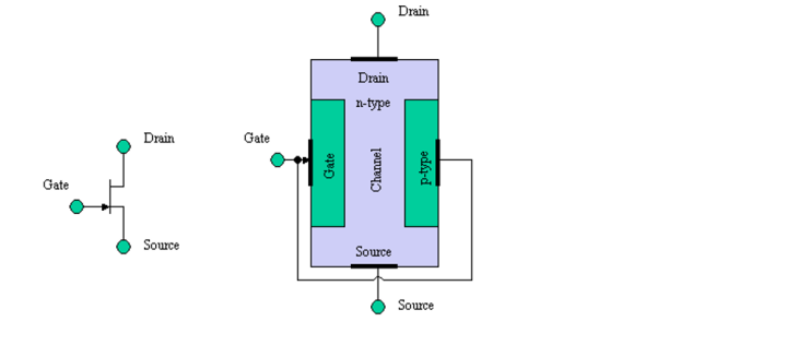
Image credit: CircuitsToday
JFETs are often used as switches or voltage-controlled resistors, and their operation can easily be compared to that of a faucet. If we consider that we can control the flow of water through a faucet by adjusting a valve, we can then compare a JFET by assigning the source terminal as the water source, the gate as the valve, and the drain as the physical drain. This means that the source contact provides the electrons which flow through the conductive channel to the drain terminal. By applying voltage to the gate, the channel becomes smaller and effectively limits the flow of electrons; this shows the JFET's use as a voltage-controlled resistor, an operation which will be described in more detail below.
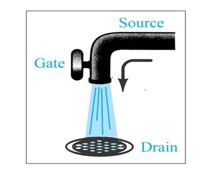
Image credit: Bolestad & Nashewski; Pearson Publishing
JFETs, like the related bipolar junction transistors (BJT), are used in a variety of modern electronic devices, such as amplifiers, switching devices, and impedance matching networks. Field effect transistors (FET) do have a number of differences when compared to BJTs, including:
- FETs are voltage-controlled; BJTs are current-controlled
- FETs have higher input impedance; BJTs have higher gain
- FETs are less sensitive to temperature variation
- FETs are unipolar, while BJTs are bipolar
Operating Principles
A JFET's operating conditions are determined by the values and changes in two different voltages: the gate-source voltage (VGS) and the drain-source voltage (VDS).
VGS = 0; VDS Increasing
If the gate-source voltage is zero (VGS=0) and the drain-source voltage is increased, three changes occur within the transistor:
- The depletion region between the n- and p-regions grows in size.
- The n-channel becomes smaller and resistance is increased.
- Despite the increased resistance, the current from the source to the drain increases due to the increasing drain-source voltage.
If the gate voltage remains at zero and the drain-source voltage continues to increase the transistor will eventually experience a pinch-off, in which the depletion layers become so thick that they close off the channel. Based on the images below, it might seem that a pinch-off would result in the drain current dropping to zero, but in this condition the drain current simply remains constant despite further increases in the drain voltage. At the pinch-off point, the drain current may be referred to as saturated (or maximized) and can be specified using the value IDSS.
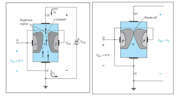
The two conditions described above: VGS=0 (left) and pinch-off.
Image credit: Bolestad and Nashewski; Pearson Publishing
Several other specifications are helpful when considering JFET operation:
- VP represents the pinch-off voltage, or the voltage necessary to induce a pinch-off condition. JFETs typically have relatively low pinch-off voltages.
- If VDS continues to increase after drain saturation has occurred, the drain current (ID) eventually begins to decrease. The gate-source voltage necessary to reduce the drain current to zero is referred to as VGS(Off).
- VDSmax specifies the maximum drain-source voltage. If this value is exceeded the drain current will increase uncontrollably, resulting in a breakdown condition and likely physical damage or destruction.
Operation as a Voltage-Controlled Resistor
Referring back to the comparison between JFETs and water faucets, the gate-source voltage can be altered to adjust the channel resistance. The graph below shows the relationship between all the variables that have been previously discussed. Note that the graph region to the left of the pinch-off voltage (VP) is known as the ohmic region.

Image credit: Bolestad and Nashewski; Pearson Publishing
Applications
JFETs are used in many of the same applications — those involving switching or amplifying — as other field effect transistors, including metal oxide semiconductor FETs (MOSFET). Due to their relatively higher transconductance properties, JFETs are especially suitable for low noise operational amplifiers.
Standards
SMD 5962-98636 — JFET Op-Amp
SMD 5962-87718 — JFET Multiplexer
Junction Field-Effect Transistors (JFET) FAQs
What are the differences between N-channel and P-channel JFETs?
Channel Type
N-channel JFETs: The channel is made of N-type semiconductor material.
P-channel JFETs: The channel is made of P-type semiconductor material.
Gate-Source Voltage (VGS) Polarity
N-channel JFETs: A negative gate-source voltage (VGS) is used to control the channel conductivity. Increasing the negative voltage enlarges the depletion region, narrowing the channel and reducing current flow.
P-channel JFETs: A positive gate-source voltage (VGS) is used to control the channel. Increasing the positive voltage has a similar effect on the depletion region and current flow as in N-channel JFETs.
Current Flow Direction
N-channel JFETs: Current flows from the drain to the source when a positive voltage is applied to the drain relative to the source.
P-channel JFETs: Current flows from the source to the drain when a negative voltage is applied to the drain relative to the source.
Commonality
N-channel JFETs: These are more commonly used due to their higher electron mobility, which generally results in better performance characteristics.
P-channel JFETs: These are less common and typically used in complementary circuits with N-channel JFETs.
How do JFETs compare to MOSFETs?
Here is a comparison between Junction Field-Effect Transistors (JFETs) and Metal-Oxide-Semiconductor Field-Effect Transistors (MOSFETs):
Structure and Material
JFETs: These transistors have a channel made of either N-type or P-type semiconductor material. The gate is formed by a PN junction.
MOSFETs: These transistors have a gate insulated from the channel by a thin oxide layer, which is why they are called metal-oxide-semiconductor FETs.
Control Mechanism
JFETs: They are voltage-controlled devices where the gate-source voltage (VGS) controls the channel conductivity. The gate is reverse-biased.
MOSFETs: Also voltage-controlled, but the gate is insulated, allowing for a higher input impedance compared to JFETs.
Input Impedance
JFETs: Have high input impedance, but generally lower than that of MOSFETs.
MOSFETs: Offer extremely high input impedance due to the insulated gate.
Applications
JFETs: Commonly used in applications requiring high input impedance and low noise, such as amplifiers and impedance matching networks.
MOSFETs: Widely used in digital and analog circuits, including power applications, due to their high efficiency and fast switching capabilities.
Performance Characteristics
JFETs: Known for their simplicity and robustness, but they have lower transconductance (current output relative to applied voltage) and voltage gain compared to MOSFETs.
MOSFETs: Provide higher transconductance and are capable of handling higher power levels, making them suitable for a wide range of applications.
Commonality
JFETs: Less common in modern integrated circuits compared to MOSFETs.
MOSFETs: Predominantly used in today's integrated circuits due to their versatility and performance advantages.
What is the function of the gate in a JFET?
The gate controls the width of the conductive channel between the source and drain. By applying a reverse-bias voltage to the gate, the current through the channel can be controlled, even to the point of completely turning it off (cutoff).
What is pinch-off voltage in a JFET?
Pinch-off voltage is the gate-source voltage at which the JFET channel becomes completely depleted, and the current between the source and drain becomes constant (saturated). Beyond this point, increasing the drain-source voltage will not increase the drain current.
How is the JFET biased?
JFETs are typically biased by applying a negative voltage to the gate with respect to the source for N-channel JFETs. This negative bias reduces the current flow through the channel. In P-channel JFETs, a positive gate-source voltage is applied.
What is the difference between depletion-mode and enhancement-mode transistors?
- Depletion-mode transistors (like JFETs) are normally on when no gate-source voltage is applied, and a reverse-bias voltage is used to turn them off or reduce current flow.
- Enhancement-mode transistors are normally off and require a positive gate-source voltage (N-channel) or negative gate-source voltage (P-channel) to turn on.
Why is the input impedance of a JFET high?
The input impedance of a JFET is high because the gate is reverse-biased, creating a depletion region, which significantly reduces the gate current. This results in very low input current, making the input impedance extremely high, often in the range of megohms.
Junction Field-Effect Transistors (JFET) Media Gallery
References
GlobalSpec—Hands-on Electronics: A One-Semester Course for Class Instruction or Self-Study