
Metal-Oxide Semiconductor FET (MOSFET) Information
Last revised: November 21, 2024
Reviewed by: Scott Orlosky, consulting engineer
Metal oxide semiconductor field-effect transistors (MOSFET) are commonly used in microprocessors and related technologies for amplifying or switching signals
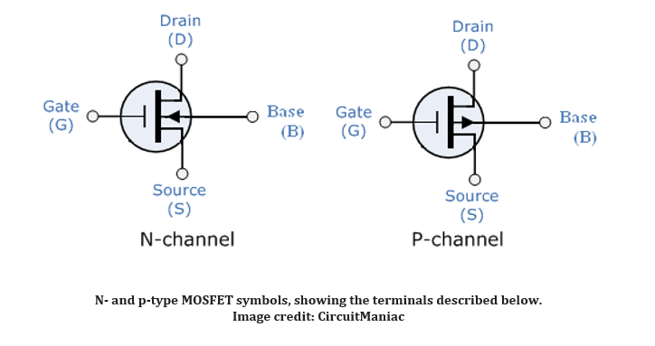
While MOSFETs technically have four terminals — source, gate, drain, and base (or body). These are usually represented by their initials (S,G,D, and B) — the base terminal is typically connected to the source, effectively making them three terminal devices like other field-effect transistors (FET). As their name implies, the MOSFET design improves upon the basic FET design by adding a layer of silicon dioxide (SiO2) to the basic substrate; this layer is represented in orange in the image below.
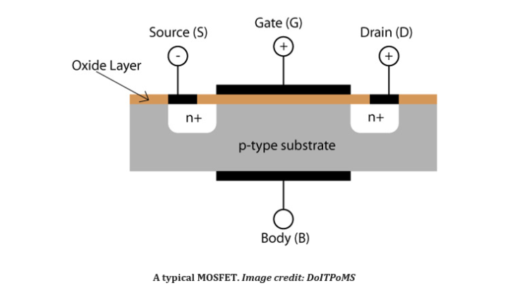
MOSFETs, like all FETs, are similar to bipolar junction transistors (BJT) with a few major differences:
- FETs are voltage-controlled as opposed to current-controlled BJTs
- FETs have higher input impedance, while BJTs have higher gain
- FETs are less sensitive to temperature changes and are better suited for IC use
- FETs are more sensitive to static than BJTs
- FETs consume less power than BJTs
- FETs are unipolar, meaning that only electrons produce the current. BJTs, as their name implies, are bipolar, meaning that electronics as well as holes produce the current.
Like all transistors, MOSFETs are commonly-used components that assist in forming the building blocks of all modern electronic devices and systems.
Specifications
Polarity
Semiconductor current conduction is facilitated by either free electrons or "holes"; both terms together can be considered as types of charge carriers. The term "hole" is used to describe the theoretical lack of an electron where one could exist in an atomic structure. Both MOSFET types described below can be of p- or n-type (also known as p-channel and n-channel), but n-channel devices are the most prevalent.
Type
MOSFETs can operate in two mode types: depletion mode (D-MOSFET) or enhancement mode (E-MOSFET).
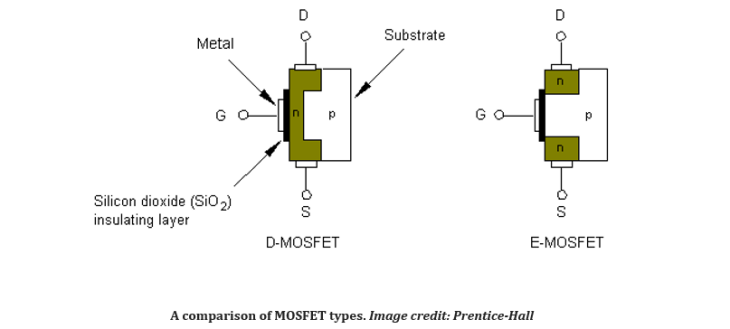
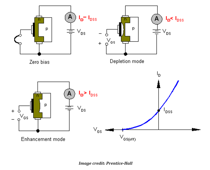
In depletion mode, the negative gate-source voltage forces free electrons away from the gate, which forms a depletion layer that cuts into the channel, as shown below. In enhancement mode, the positive gate-source voltage attracts electrons from the substrate to the channel while driving holes away from the channel. This process results in a wider channel and results in a smaller steady current and larger drain current, compared to the larger current of depletion mode. MOSFETs can also operate in a zero bias state in which the gate is shorted to the source terminal, meaning that the transistor's drain current is equal to its steady state current. All three of these states, as well as a graph describing gate voltage's effect on the transistor's steady state current, are shown below.
D-MOSFET
Depletion MOSFETs have a gate channel — created by doping impurities into the p-type substrate — between the drain and the source terminals, both of which are connected to the n-type materials, which in turn lie on a p-type substrate. A D-MOSFET can operate in both depletion and enhancement modes, while an E-MOSFET, described below, can only operate in enhancement mode. As shown above, a D-MOSFET's primary difference from an E-type is that its drain and source terminals are connected by an n-type channel.
E-MOSFET
E-MOSFETs lack a built-in channel. Instead the drain and source terminals are created by doping the source and drain regions with n-type material. However, an n-type channel will form between the terminals if a positive voltage is applied between the gate and the source. E-MOSFETs are sometimes regarded as the most important type of MOSFET because of their ease of manufacture and outstanding switching and amplifying characteristics. P- and n-type E-MOSFETs can be combined to produce Complementary Metal Oxide Semiconductor (CMOS) devices.
Numerical Specifications
When discriminating between different MOSFET products, two important specifications to consider include drain saturation current and gate-source cutoff voltage.
Drain saturation current (IDSS) is a measure of drain current saturation, a condition that occurs when the drain-source voltage equals the gate-source voltage. When a MOSFET's drain current reaches a maximum value it remains there despite any increases in the drain-source voltage; this extra voltage is accommodated by a depletion layer located at the drain end of the gate. This condition is known as drain current saturation, and is represented by IDSS as a maximum current value.
Gate-source cutoff voltage (VGS(Off)) represents the value of the gate-source voltage (VGS) which results in a drain current (ID) value of close to zero.
Metal-Oxide Semiconductor FET (MOSFET) FAQs
What is the impact of gate capacitance on MOSFET performance?
Gate capacitance affects the current and slew rate needed to turn the gate on and off. This directly impacts the switching speed of the MOSFET. The equation that governs this relationship is: I = C (dV/dt) where ( I ) is the current, ( C ) is the gate capacitance, and ( dV/dt) is the rate of change of voltage. A higher gate capacitance requires more current to achieve the same switching speed, which can slow down the switching process.
The total gate charge, which is related to gate capacitance, determines the upper-frequency limit of the MOSFET's switching speed. A lower total gate charge is preferred for efficient switching, as it allows the MOSFET to operate at higher frequencies with less power loss.
When designing circuits with MOSFETs, it's crucial to balance the gate capacitance with the drive capability of the circuit. This ensures that the MOSFET can switch efficiently without excessive power dissipation or slow response times.
These factors highlight the importance of considering gate capacitance when selecting a MOSFET for specific applications, as it plays a crucial role in determining the device's overall performance and efficiency.
What is the relationship between gate capacitance and total gate charge?
Gate capacitance is a measure of the MOSFET's ability to store charge at the gate terminal. It affects the current and slew rate needed to turn the gate on and off, which directly impacts the switching speed of the MOSFET. The switching speed is represented by the formula I = C (dV/dt).
Total gate charge is the total amount of charge required to switch the MOSFET from the off state to the on state. It is directly related to the gate capacitance and determines the upper-frequency limit of the MOSFET's switching speed. A lower total gate charge is preferred for efficient switching, as it allows the MOSFET to operate at higher frequencies with less power loss.
The total gate charge is essentially the integral of the gate capacitance over the voltage range required to switch the MOSFET. It represents the cumulative effect of the gate capacitance over the entire switching process. Therefore, while gate capacitance affects the instantaneous current required for switching, the total gate charge provides a measure of the overall energy required to complete the switching cycle.
Understanding this relationship is important for designing circuits that require fast and efficient switching, as it helps in selecting MOSFETs that match the drive capability of the circuit without excessive power dissipation or slow response times.
How does gate capacitance affect power dissipation in MOSFETs?
The impact of gate capacitance on power dissipation in MOSFETs is an important consideration in their performance and efficiency.
Gate capacitance influences the amount of current required to charge and discharge the gate during switching. The equation governing this relationship is: I = C (dV/dt) I is the current, ( C ) is the gate capacitance, and (dV/dt) is the rate of change of voltage. Higher gate capacitance requires more current to achieve the same switching speed, means increased power dissipation during the switching process.
The total gate charge (Qg) is directly related to gate capacitance and determines the energy required to switch the MOSFET from off to on. A higher total gate charge means more energy is consumed during each switching cycle, leading to increased power dissipation.
Lower gate capacitance and total gate charge are preferred for efficient switching, as they reduce the energy required for each switching event. This results in lower power dissipation and improved overall efficiency of the MOSFET.
In summary, gate capacitance affects power dissipation primarily through its impact on switching losses and the total energy required for gate charge. Selecting MOSFETs with lower gate capacitance and total gate charge can help minimize power dissipation increase switching time and enhance efficiency.
What are some methods to reduce power dissipation in MOSFETs?
To reduce power dissipation in MOSFETs, several methods can be employed, focusing on minimizing switching losses and optimizing the device's efficiency.
Lower On-Resistance (RDS(on))
Selecting MOSFETs with lower on-resistance can significantly reduce resistive losses and voltage drop when the device is conducting. This leads to decreased power dissipation and increased efficiency.
Minimize Gate Capacitance and Total Gate Charge (Qg)
Reducing the gate capacitance and total gate charge helps in minimizing the energy required for each switching cycle. This results in lower power dissipation during the switching process.
Efficient Switching Performance
Opt for MOSFETs with excellent switching performance, characterized by low gate charge and fast switching capabilities. This reduces the time the MOSFET spends in the transition state, thereby minimizing switching losses.
Optimized Drive Circuit
Design the drive circuit to match the MOSFET's gate capacitance, ensuring efficient charging and discharging of the gate. This helps in reducing the power consumed during switching.
Use of Advanced MOSFET Designs
Consider using advanced MOSFET designs that offer reduced on-resistance and improved efficiency. These designs can handle higher currents with lower power dissipation.
These methods focus on optimizing the MOSFET's performance to reduce power dissipation, thereby enhancing the overall efficiency of the application.
What is the impact of on-resistance on MOSFET efficiency?
The impact of on-resistance (RDS(on)) on MOSFET efficiency is a critical factor to consider when selecting a MOSFET for specific applications. Lower on-resistance means that there is less resistive loss and voltage drop when the MOSFET is conducting. This directly translates to reduced power dissipation (I2R losses) and increased efficiency, as less energy is wasted as heat during operation.
By minimizing on-resistance, the MOSFET can handle higher currents more efficiently. This is particularly important in applications where the MOSFET is required to conduct large amounts of current, as even small resistive losses can lead to significant power dissipation.
Advances in MOSFET design have led to reductions in on-resistance to very low levels, often in the range of tens of milliohms. This improvement helps in maintaining high efficiency even when the MOSFET is used in high-current applications.
Conduction losses, which occur when the MOSFET is in the on-state, are directly proportional to the on-resistance. Therefore, selecting a MOSFET with a low RDS(on) is crucial for applications that require high efficiency and low heat generation.
In summary, the on-resistance of a MOSFET is a key determinant of its efficiency, especially in high-current applications. Lower on-resistance leads to reduced power dissipation, improved efficiency, and better overall performance.
What are some advanced MOSFET designs that offer reduced on-resistance?
Advances in MOSFET design have significantly reduced on-resistance to very low levels, (tens of milliohms). This reduction is crucial for applications that require handling high currents efficiently, as it minimizes resistive losses and improves overall efficiency
An example of an advanced MOSFET design is the PolarP P-Channel enhancement mode power MOSFET. This device features a low on-state resistance of 4.2 Ω, which helps in reducing power dissipation and heat generation, thereby improving efficiency in end applications. It also offers excellent switching performance with a low gate charge, allowing for fast and efficient operation.
These advanced designs focus on minimizing on-resistance to enhance efficiency and performance, particularly in high-current applications.
The PolarP MOSFET features a low on-state resistance which reduces power dissipation and heat generation, improving efficiency.
A further improvement to switching performance comes with a low gate charge of 11.9 nC. This allows for fast and efficient switching.
The PolarP MOSFET is designed to withstand harsh conditions, thanks to its dynamic dv/dt and avalanche rating. This makes it a reliable choice for demanding operating environments, particularly in automotive applications where durability is crucial.
Metal-Oxide Semiconductor FET (MOSFET) Media Gallery
References
GlobalSpec—RF MOSFET Transistors
Georgia State University—MOSFETs
University of Colorado—MOS Field-Effect Transistors
Image Credit: