RF Transistors Information
Last revised: December 5, 2024
Reviewed by: Scott Orlosky, consulting engineer
RF transistors are designed to handle high-power radio frequency (RF) signals in devices such as:
- Stereo amplifiers
- Radio transmitters
- Television monitors
Like other semicon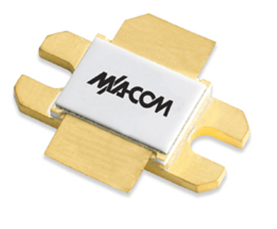 ductor devices, they are made of materials such as silicon (Si) or germanium (Ge) and doped with impurities to induce changes in electrical properties.
There are several basic types of RF transistors:
- Bipolar RF transistors: Consist of an N-type or P-type layer sandwiched between two layers of the opposite type. Both NPN and PNP configurations are available.
- MOSFET RF: Metal-oxide field effect transistors (MOSFETs) with a channel made of either an N-type or P-type material.
- Heterojunction field effect transistors (HFETs): Require a negative power supply and are used mainly for driver or power amplification applications.
- Pseudomorphic high electron mobility transistors (PHEMTs): Used mainly in wireless devices and satellite communication systems.
Specifications
Selecting RF transistors requires an analysis of performance specifications. Power gain, a measure of power amplification, is the ratio of output power to input power.
Noise figure, a measure of the amount of noise added during normal operation, is the ratio of the signal-to-noise ratio at the input and the signal-to-noise ratio at the output.
Both power gain and noise figure are expressed in decibels (dB).
Other performance specifications for RF transistors include:
- Output power
- Operating frequency
- Operating temperature
Some RF transistors support a temperature range and feature mechanical and electrical specifications that are suitable for commercial or industrial applications. Other devices meet screening levels for military specifications (MIL-SPEC).
IC Package Types
Basic integrated circuit (IC) package types for RF transistors are:
- Transistor outline (TO)
- Small outline (SO)
- Small outline transistor (SOT)
For each package type, many variants are available. Transistor outline packages include:
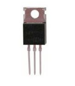
- TO-92: A single in-line package often used for low power devices.
- TO-220: Suitable for high power, medium current, and fast-switching power devices.
- TO-263: The surface-mount version of the TO-220 package.
Small outline transistor packages include:
- SOT23: Often used in home appliances, office and industrial equipment, personal computers, printers, and communication equipment.
- SOT89: A plastic, surface mounted package with three leads and a collector pad for good heat transfer.
- SOT223: An encapsulated package that provides excellent performance in environments with high temperatures and humidity levels.
IC package types that use flat packaging (FPAK) are also available.
Packing Methods
Packing methods for RF transistors consist of:
- Tape reel
- Rail
- Bulk pack
- Tube technologies
The tape reel method packs components in a tape system by reeling specified lengths or quantities for shipping, handling, and configuration in industry-standard automated board-assembly equipment.
Rail, another standard packing method, is typically used only in production environments. Bulk pack devices are distributed as individual parts, while some components are designed to be shipped in trays.
Typically, the tube or stick magazine method is used to feed bipolar RF transistors into automatic placement machines for through-hole or surface mounting.
Standards
BS EN 120003 — Specification for harmonized system of quality assessment for electronic components — blank detail specification — phototransistors, photodarlington transistors, phototransistor arrays.
BS EN 62373 — Bias-temperature stability test for metal-oxide, semiconductor, field-effect transistors (MOSFET).
RF Transistors FAQs
What are the differences between Bipolar Junction Transistors (BJTs) and Field-Effect Transistors (FETs)?
- Control Mechanism: BJTs are current-controlled, while FETs are voltage-controlled.
- Gain and Impedance: BJTs typically offer higher gain, whereas FETs have higher input impedance.
- Power Consumption: BJTs generally consume more power than FETs.
- Sensitivity to Static: BJTs are less sensitive to static compared to FETs.
- Polarity: BJTs are bipolar devices, while FETs are unipolar.
What are the advantages of using MOSFETs over BJTs in RF applications?
MOSFETs have higher input impedance compared to BJTs, which can be beneficial in certain applications. MOSFETs generally consume less power than BJTs. MOSFETs are voltage-controlled devices, which can simplify the design of certain circuits. MOSFETs can switch faster than BJTs, making them suitable for high-frequency applications.
What are the disadvantages of using MOSFETs in RF applications?
MOSFETs are more sensitive to static electricity compared to BJTs. Designing circuits with MOSFETs can be more complex due to their voltage control characteristics.
How do the specifications of RF transistors impact their performance in different applications?
For RF power transistors, manufacturers typically specify large-signal input and output impedances instead of small-signal parameters like Y and S parameters. These impedances are crucial for designing matched amplifiers, where the input and output impedances are conjugately matched to the source and load, respectively. This matching is essential for optimal power transfer and efficiency in RF power amplifiers.
The noise figure (NF) is a measure of the noise added by the transistor during operation. It is particularly important in applications like the front end of a microwave satellite receiver system, where low noise is critical for signal clarity. The noise figure is frequency-dependent, and selecting a transistor with an appropriate NF for the operating frequency is essential for minimizing noise in sensitive applications.
Power gain, the ratio of output power to input power, is a critical specification for amplifiers. It is expressed in decibels (dB) and can be specified in different ways, such as maximum allowable gain (Gmax) or gain at optimum noise figure (GNF). High power gain is essential for applications requiring significant signal amplification, such as RF amplifiers and broadcast equipment.
This specification indicates the maximum voltage the transistor can handle between the drain and source before breakdown occurs. It is critical for ensuring the transistor can operate safely within the voltage limits of the application, particularly in high-power or high-voltage environments.
Power dissipation, measured in watts (W) or milliwatts (mW), indicates the total power consumed by the transistor. It is an important factor in thermal management and efficiency, especially in applications where power consumption needs to be minimized.
The operating frequency range of the transistor determines its suitability for different RF applications. For instance, transistors used in satellite radio or navigation systems need to operate efficiently at specific frequency bands like Ku or Ka bands.
Bipolar Junction Transistors (BJTs) and Field-Effect Transistors (FETs) have different characteristics. BJTs are current-controlled and typically offer higher gain but consume more power, making them suitable for high-gain applications. FETs, being voltage-controlled and having higher input impedance, are preferred in applications requiring low power consumption and high input impedance.
The performance of RF transistors in different applications is heavily influenced by their specifications, including large-signal impedances, noise figure, power gain, breakdown voltage, power dissipation, operating frequency, and the type of transistor. Selecting the right transistor with appropriate specifications will optimize performance in specific RF applications.
What is the importance of noise figure in RF transistors?
The noise figure of RF transistors is a specification that significantly impacts their performance, especially in applications where signal clarity and low noise are paramount.
The noise figure is a measure of the noise added by the transistor during its operation. It is defined as the ratio of the signal-to-noise ratio (SNR) at the input to the SNR at the output, expressed in decibels (dB).
Noise figure is highly frequency-dependent. When selecting a transistor, it is essential to consult the NF-vs-frequency curve to ensure that the noise figure is appropriate for the operating frequency of the application. Device data sheets often list the maximum frequency and minimum noise figure, but these two parameters rarely coincide, so careful consideration is needed.
In receiver systems, such as the front end of a microwave satellite receiver, the noise figure is very important. A low noise figure will maintain signal clarity and minimize the noise introduced by the transistor. This is particularly important in applications like earth communications or receiver terminals, where a low-noise amplifier (LNA) is used at the feedpoint of a parabolic dish antenna.
Different applications may prioritize noise figure differently. For example, in the front ends of receiver systems, both gain and noise figure are important. However, in other applications, power gain and output might be more important. Selecting a transistor with an appropriate noise figure for the specific application is necessary for optimal performance.
When designing RF circuits, the noise figure must be considered alongside other specifications such as power gain, breakdown voltage, and power dissipation. The goal is to achieve a balance that meets the performance requirements of the application while minimizing noise.
In summary, the noise figure is a vital specification for RF transistors, particularly in applications where low noise is critical for signal clarity. It is essential to consider the frequency dependence of the noise figure and select transistors that provide an appropriate balance of noise figure and other performance characteristics for the specific application.
How do large-signal input and output impedances affect the design of RF power amplifiers?
In RF power amplifiers, the input and output impedances of the transistor are conjugately matched to the source and load, respectively. This means that the reactive part of the impedance is canceled out, and the resistive part is transformed for maximum power transfer. This matching is essential for achieving optimal power transfer and efficiency in the amplifier.
When designing an RF power amplifier, the large-signal input and output impedances are specified instead of small-signal parameters like Y and S parameters. These impedances are measured when the device operates as a matched amplifier at the desired DC supply voltage and RF power output level.
Proper impedance matching ensures that the maximum amount of power is transferred from the source to the load. This is particularly important in high-power applications where efficiency carries more weight in the design.
Matching the impedances also helps in maintaining the stability and linearity of the amplifier, which are essential for high-quality signal amplification.
RF power transistor data sheets typically present large-signal input and output impedances. This information is necessary for circuit designers to achieve the desired performance characteristics in their designs.
Some data sheets include both series- and shunt-impedance information. This provides designers with the flexibility to use different matching techniques to optimize the amplifier's performance
In summary, large-signal input and output impedances are fundamental to the design of RF power amplifiers. They ensure optimal power transfer, stability, and efficiency by enabling proper impedance matching between the transistor, source, and load. Designers rely on these specifications to achieve the desired performance in their RF amplifier circuits.
RF Transistors Media Gallery
References
GlobalSpec—RF MOSFET Transistors
GlobalSpec—Secrets of RF Circuit Design, Third Edition
GlobalSpec—RF Circuit Design, Second Edition
Image Credits:
MACOM | TT Semiconductor, Inc. | 1-Source Electronic Components