
Bipolar RF Transistors Information
Last revised: January 8, 2025
Reviewed by: Scott Orlosky, consulting engineer
Bipolar RF transistors are designed to handle high power radio frequency (RF) signals in amplifiers, transmitters, monitors, and other devices. Like all transistors, they are used to switch and amplify signals in digital and analog circuits.
Basic Principles
Construction
Bipolar transistors, also referred to as bipolar junction transistors (BJT), are produced by stacking three layers of semiconductor material. The two different types of material, both of which are capable of conducting current, are referred to as n- and p-type materials. N-type semiconductors operate using excess free electrons, while p-types use excess "holes." In this context a hole is simply the lack of an electron where one could theoretically exist. By stacking layers of p- and n-type materials, semiconductors form multiple p-n junctions, which can be utilized for their various electrical properties.
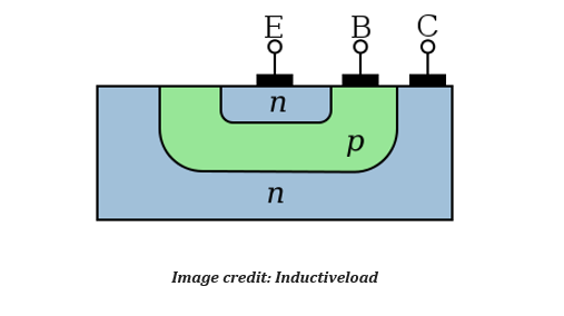
Based on the principles above, bipolar transistors can be one of two types: NPN (a p-region sandwiched between two n-regions) or a PNP (the opposite of an NPN). The current and voltage polarities of an NPN transistor are opposite those of PNP and vice versa. NPNs are the most widely used bipolar transistors and will be discussed in detail. Each layer or region is connected to a different terminal; the layers and terminals are designated as base (B), emitter (E), and collector (C). The image below shows the cross-section of a basic NPN transistor, complete with labeled terminals.
Operation
A primary use for bipolar transistors is to control the output collector current (IC) by varying the current ("current-controlled") or voltage ("voltage-controlled") of the base terminal. Because a very small current or voltage at the base terminal can result in a much larger collector output, bipolar transistors often function as current amplifiers. Current gain represents the factor of current amplification is an important specification relative to this function. While manufacturers typically specify this value, it can also be calculated using the following formula:
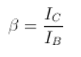
where:
β = current gain factor
IC = collector current
IB = base current
A bipolar transistor's ability to amplify signals is based on its n- and p-doped regions. In basic terms, when a positive bias (charge or voltage) is applied to the base terminal, it forces the holes inherent in the p-region toward the emitter terminal and allows excited electrons to be swept from the n-type emitter region to the collector terminal, resulting in a relatively high current output. This action is shown in the image below.
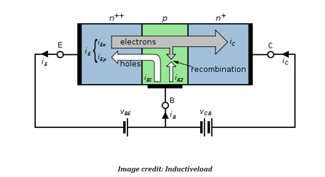
When a transistor operates in this manner, it is said to be in an active state. Bipolar transistors can also function in two other states:
- Cut-off: the device has no output.
- Saturated: the collector output has reached its maximum value. Any increases in the base terminal's current or voltage will not affect the device's output.
Transistor Configurations
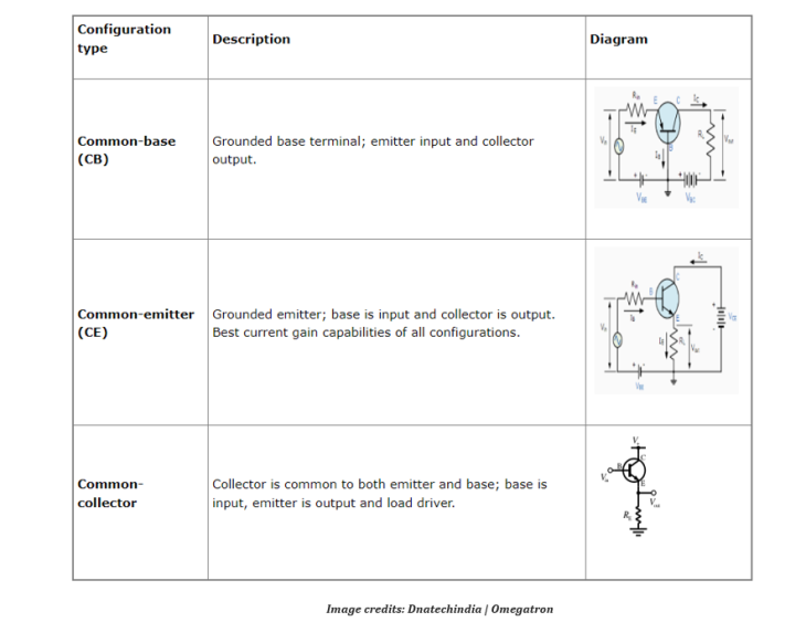
When transistors are used in circuits, one of the terminals must be grounded. Based on this fact, there are three possible transistor configurations, all of which are shown in the table below.
Bipolar Transistors Versus Field-Effect Transistors
Bipolar transistors are often compared with field-effect transistors (FET); each of these devices have inherent advantages and differences.
- BJTs are typically current-controlled, vs. voltage-controlled FETs
- BJTs are capable of higher gain, while FETs have higher impedances
- BJTs typically consume more power
- BJTs are less sensitive to static than FETs
- FETs are unipolar, while BJTs are bipolar
Applications
Transistors are the building block of all major electronics and are used in an enormous variety of applications and industries. Bipolar RF transistors are useful as switches and amplifiers in any device that uses radio frequency (RF) signals. Examples of these devices include:
- RF amplifiers
- Radios and other communication equipment
- Cellular phones
- Broadcast equipment
- Avionics equipment
Specifications
Numerical Specs
As mentioned above, a transistor's collector output current (IC) is typically specified by the manufacturer and is one of the most important numerical specifications. Other specifications include breakdown voltage, output power, and power dissipation.
- Breakdown voltage is the maximum voltage a device can sustain without physical damage or destruction. Buyers of bipolar RF transistors may consider the collector-emitter breakdown voltage (VCEO) and the collector-base breakdown voltage (VCBO).
- Output power represents the total power produced by the transistor, measured in watts (W).
- Power dissipation is the total power consumed by the transistor, expressed in watts or milliwatts (mW). Because bipolar transistors are easily destroyed by heat, it is extremely important to note how much power a device can dissipate without sustaining damage.
Numerical specifications unique to radio frequency (RF) devices include operating frequency (in Hz, kHz, or MHz), unity gain bandwidth, and noise figure (NF).
Unity gain bandwidth refers to the frequency at which an RF transistor's current gain is unity.
Noise figure (NF) is the ratio, in decibels (dB), of two other ratios: the signal-to-noise ratio at the input and the signal-to-noise ratio at the output. NF is basically expressed as the amount of noise added to a signal during normal operation. Lower noise figures result in better device performance.
Standards
The manufacturing and testing of bipolar RF transistors is covered by numerous standards. Common standards include:
BSI - BS EN 60747-16-1—Microwave ICs: amplifiers
NPFC - MIL-S-19500/27 —High frequency PNP transistors
Bipolar RF Transistors FAQs
What are the common standards for testing RF amplifiers?
Here are some common standards for testing RF amplifiers:
Noise Figure Testing
The standard for noise figure testing of RF amplifier tubes comes from ECIA - EIA TEP 138 and is outlined in TEP 38. This standard is used for assessing the noise performance of RF amplifiers, a key parameter in determining efficiency and effectiveness in amplifying weak signals.
Radio Frequency Power Testing
Standards such as RF Power Amplifier Testing cover the testing of RF power from 50 MHz to 26.5 GHz and 50 MHz to 40 GHz. These standards are essential for ensuring that RF amplifiers meet the required power output specifications
High Power Amplifiers
The standard for methods of measurement for equipment used in digital microwave radio transmission systems includes measurements on satellite earth stations and high power amplifiers. This standard is important for testing the performance of high power RF amplifiers used in satellite communications.
Active Antenna Amplifier Tests
The "Active Antenna Amplifier Electrical Characteristics Tests" standard specifies requirements and test procedures for verifying the performance of active antenna systems, which include RF amplifiers. This standard is applicable to various frequency bands and is used to ensure the reliability and performance of antenna systems in vehicles.
These standards help ensure that RF amplifiers are tested for performance, reliability, and compliance with industry requirements.
What is the role of noise figure testing of RF amplifiers?
Noise figure testing of RF amplifiers is an important process to assess the noise performance of these devices. This testing established if the system meets the performance necessary to meet their efficiency and effectiveness in amplifying weak signals. Here are some key points about noise figure testing:
The noise figure test measures the noise performance of an RF amplifier. It quantifies how much noise the amplifier adds to the signal it processes, which is critical for applications where signal clarity and strength are paramount.
A lower noise figure indicates better performance, as it means the amplifier adds less noise to the signal. This is particularly important in communication systems where signal integrity is essential.
How do the basic principles of bipolar RF transistors differ from other types of transistors?
The basic principles of bipolar RF transistors differ from other types of transistors, such as field-effect transistors (FETs), in several ways.
Control Mechanism
Bipolar junction transistors (BJTs) are current-controlled devices. This means that the output current is controlled by the input current at the base terminal.
In contrast, FETs are voltage-controlled devices, where the output current is controlled by the input voltage at the gate terminal.
Charge Carriers
BJTs are bipolar devices, meaning that the current through the transistor is carried by both holes (positive charge carriers) and electrons (negative charge carriers).
FETs, on the other hand, are unipolar devices, where the current is carried by either electrons or holes, but not both.
Gain and Impedance
BJTs are capable of higher gain compared to FETs. This makes them suitable for applications requiring amplification of weak signals.
FETs have higher input impedance, which can be advantageous in applications where minimal loading of the preceding stage is desired.
Power Consumption and Sensitivity
BJTs typically consume more power than FETs. This is due to the continuous base current required to maintain the transistor in the 'on' state.
BJTs are less sensitive to static electricity compared to FETs, which can be a consideration in certain environments.
Applications
Bipolar RF transistors are particularly useful in applications involving radio frequency signals, such as RF amplifiers, radios, cellular phones, and broadcast equipment.
What is the difference between n-p-n and p-n-p bipolar transistors?
The differences between n-p-n and p-n-p bipolar transistors are primarily based on their construction and operation.
Construction
For a n-p-n Transistor: This type of bipolar junction transistor (BJT) is constructed with a thin layer of p-type semiconductor sandwiched between two n-type semiconductors. The current flows from the collector to the emitter when a positive voltage is applied to the base relative to the emitter.
For a p-n-p Transistor: In contrast, a p-n-p transistor consists of a thin layer of n-type semiconductor between two p-type semiconductors. The current flows from the emitter to the collector when a negative voltage is applied to the base relative to the emitter.
Operation
For a n-p-n Transistor: In an n-p-n transistor, the majority charge carriers are electrons. When the base-emitter junction is forward-biased, electrons are injected from the emitter into the base, where they are minority carriers. These electrons then move to the collector, creating a current flow.
For a p-n-p Transistor: For a p-n-p transistor, the majority charge carriers are holes. When the base-emitter junction is forward-biased, holes are injected from the emitter into the base, where they are minority carriers. These holes then move to the collector, facilitating current flow.
Biasing
For a n-p-n Transistor: Requires a positive voltage at the base relative to the emitter to turn on.
For a p-n-p Transistor: Requires a negative voltage at the base relative to the emitter to turn on.
These structural and operational differences influence how each type of transistor is used in circuits, with n-p-n transistors being more common in applications where a positive supply voltage is used, and p-n-p transistors being used in circuits with a negative supply voltage.
What are the advantages of using BJTs in communication equipment?
The advantages of using Bipolar Junction Transistors (BJTs) in communication equipment are primarily due to their specific characteristics which make them well-suited to these applications as expanded down below.
High Gain
BJTs are capable of providing high gain, which is essential for amplifying weak radio frequency (RF) signals. This high gain is particularly beneficial in communication equipment where signal strength needs to be increased significantly to ensure clear and reliable communication.
Robustness
BJTs are less sensitive to static electricity compared to Field-Effect Transistors (FETs). This robustness is advantageous in communication equipment where reliability is critical, as it reduces the risk of damage from static discharge.
Versatility in Applications
BJTs are commonly used in various communication devices such as radios and cellular phones. In these applications, they serve as RF amplifiers to enhance signal quality and strength, ensuring effective communication over different distances and conditions.
Bipolar RF Transistors Media Gallery
References
All About Circuits—Bipolar Junction Transistors
GlobalSpec—Noise Figure Testing of RF Amplifier Tubes (TEP 38)