Power MOSFET Information
Last revised: November 24, 2024
Reviewed by: Scott Orlosky, consulting engineer
Power MOSFETs are specialized metal oxide semiconductor field-effect transistors (MOSFET) designed to handle significant power levels.
Although early power MOSFET manufacturing used several different designs, the Vertical Diffused MOS (VDMOS) — also known as the Double-diffused MOS (DMOS) — emerged as the predominate design. The terms "vertical" and "diffusion" are adequate to describe the construction of a power MOSFET. "Vertical" refers to the fact that, unlike traditional (or "lateral") MOSFETs, a power MOSFET's source terminal is above its drain terminal, resulting in a primarily vertical current. By contrast, a lateral MOSFET's source and drain terminals are on opposite sides of the device, with the gate situated on the n-doped channel. "Diffusion" refers to the device's manufacturing process: the p-type and n-type wells that sit on the n-type substrate are created using a double-diffusion process.
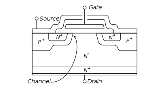
A VDMOS diagram, showing its vertical construction and N+ and P+ wells. Image credit: Wikipedia
Despite the predominance of VDMOS, some lateral power MOSFETs are still used in specialized applications.
Power MOSFET operation is slightly different than that of a lateral e-MOSFET. In lateral MOSFETs, planar construction results in current and breakdown voltage values which are functions of the channel dimensions, rendering the device relatively inefficient. In contrast, the vertical construction of power MOSFETs results in voltage ratings which are functions of the doping and thickness of the n-type well, while current rating remains a function of channel width. Power MOSFETs are therefore able to sustain high voltages and high currents without increasing the size of the device.
Power MOSFETs are used in many applications necessitating power semiconductors. Compared to insulated-gate bipolar transistors (IGBT) and thyristors, power MOSFETs feature very high switching speeds and improved efficiency at low voltages. Power MOSFETs are the most common low-voltage (less than 200 V) switch in use, and can be found in power supplies, DC-DC converters, and controllers.
Operating Principles and Specifications
Like all MOSFETs, power MOSFETs switch and regulate a current that flows between the source (S) and drain (contacts) by varying voltage at the gate (G) terminal. By applying a voltage to the gate, a channel is created between the gate and the source, allowing current to flow.
By increasing the gate-source voltage (VGS), the channel becomes larger and the drain current (ID) increases. The relationship between the gate voltage and drain voltage is dependent upon the following equation:
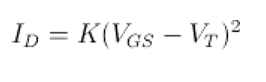
where:
ID = drain current
K = device constant
VGS = gate voltage
VT = threshold voltage
Threshold voltage (VT) refers to the minimum voltage necessary to create a channel. By visually plotting a device's drain current against its various gate-source voltages we can determine the device's transfer characteristics. A graphical representation of a typical n-channel power MOSFET's transfer characteristics is shown below.
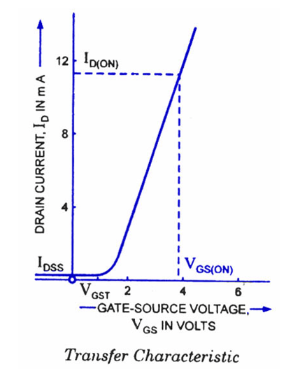
Image credit: Circuitstoday
Other Specifications
When selecting power MOSFET products, two important specifications to consider include drain saturation current and gate-source cutoff voltage.
Drain saturation current (IDSS) is a measure of drain current saturation, which occurs when the drain-source voltage equals the gate-source voltage. When a MOSFET's drain current reaches a maximum value it remains there despite any increases in the drain-source voltage; this extra voltage is accommodated by a depletion layer located at the drain end of the gate. This condition is known as drain current saturation, and is represented by IDSS as a maximum current value.
Gate-source cutoff voltage (VGS(Off)) is the value of the gate-source voltage (VGS) which results in a drain current (ID) value of close to zero.
Standards
Power MOSFETs can be manufactured and tested using standards developed by a diverse range of societies and associations. Examples include:
- JEDEC JEP 115 — Power MOSFET Electrical Dose Rate Test Method
- BSI-BS IEC 60747-8-4 — MOSFETs for power switching applications
- JEDEC JESD 24 — Power MOSFETs
Power MOSFETs FAQ
What is on-resistance (RDS(on)) and why is it important?
On-resistance is the resistance between the drain and source when the MOSFET is in the "on" state. Lower on-resistance means reduced resistive loss and voltage drop when conducting, leading to increased efficiency. Advances in MOSFET design have reduced on-resistance to tens of milliohms.
What role does gate capacitance play in MOSFET performance?
Gate capacitance determines the current and slew rate needed to turn the gate fully on and off with the desired transition time, which relates to switching speed. The equation governing this is I = C (dV/dt ).
What are some specialized types of power MOSFETs?
Super-Junction MOSFETs are known for fast operation and low noise, and they offer considerable variety. Meanwhile, SiC-MOSFETs use silicon carbide and are known for their high efficiency and performance in high-temperature environments.
What are the latest advancements in power MOSFET technology?
Advances in MOSFET design have significantly reduced on-resistance to tens of milliohms. This reduction is crucial for handling high currents with minimal resistive loss and voltage drop, leading to increased efficiency in power applications.
Enhancements in gate capacitance have been made to optimize the current and slew rate needed to turn the gate fully on and off with the desired transition time. This improvement directly impacts the switching speed and overall performance of the MOSFET.
Super-junction MOSFETs have seen continuous improvements, particularly in fast operation and low noise characteristics. These advancements provide a considerable variety of options for different applications, enhancing the versatility and performance of these devices.
SiC-MOSFETs are known for their high efficiency and superior performance in high-temperature environments. The use of silicon carbide as a material allows these MOSFETs to operate more efficiently and reliably under demanding conditions.
The introduction of automotive-grade MOSFETs, such as the PolarP P-Channel enhancement mode power MOSFET, has brought significant advancements. These MOSFETs offer low conduction loss, excellent switching performance, and ruggedness in demanding environments, making them suitable for automotive applications that require durability and reliability.
These advancements highlight the ongoing improvements in power MOSFET technology, making them more efficient, reliable, and versatile for a wide range of applications.
What is the reduction in on-resistance in power MOSFETs?
The reduction in on-resistance (RDS(on)) in power MOSFETs is a significant advancement that has greatly improved their efficiency and performance. Here are some key points about this reduction:
On-resistance (RDS(on)) is the resistance between the drain and source when the MOSFET is in the "on" state. Lower on-resistance means reduced resistive loss and voltage drop when conducting, which leads to increased efficiency and reduced power dissipation. These advancements in reducing on-resistance have made power MOSFETs more efficient and reliable, making them suitable for a wide range of applications, from power supplies to automotive systems.
Advances in MOSFET design have significantly reduced on-resistance leading to increased efficiency in power applications.
Continuous improvements in semiconductor materials and fabrication techniques have contributed to the reduction in on-resistance. Super-junction MOSFETs and SiC-MOSFETs have further pushed the boundaries of efficiency and performance
Power MOSFETs Media Gallery
References
Fairchild Semiconductor—Introduction to Power MOSFET (pdf)
Georgia State University—MOSFETs
University of Colorado—MOS Field-Effect Transistors
Image Credit:
Advanced Power Electronics Corp. | RS Components | Mouser Electronics