DRAM and SDRAM Memory Chips Information
Last revised: February 25, 2025
Dynamic random access memory (DRAM) chips are single-transistor memory cells that use small capacitors to store each bit of memory in an addressable format that consists of rows and columns. Because capacitors are unable to hold a charge indefinitely, DRAM memory chips require a near-constant pulse of current to retain stored information. If DRAM memory chips are not refreshed, data is lost. Though less expensive than synchronous random access memory (SRAM), DRAM requires extra processing time to restore the contents of memory addresses. DRAM is used widely in personal computers and workstations. Common DRAM types include extended fast page mode (FPM) DRAM and extended operation (EO) DRAM.
Specifications
DRAM memory chips vary in terms of density, number of words, bits per word, internal blanks, supply voltage, and operating temperature.
- Density is the capacity of the chip in bits.
- The number of words equals the number of rows, each of which stores a memory word and connects to a word line for addressing purposes.
- The bits per word are the number of columns, each of which connects to a sense / write circuit.
- Supply voltages range from - 5 V to 5 V and include intermediate voltages such as -4.5 V, -3.3 V, -3 V, 1.2 V, 1.5 V, 1.8 V, 2.5 V, 3 V, 3.3 V, and 3.6 V.
- Some DRAM memory chips support a specific temperature range and feature mechanical and electrical specifications that are suitable for commercial or industrial applications.
- Other DRAM memory chips meet screening levels for military specifications (MIL-SPEC).
Selection Criteria
Selecting DRAM memory chips requires an analysis of performance specifications such as access time, refresh rate, and refresh options.
- Measured in nanoseconds (ns), access time indicates the speed of memory and represents a cycle that begins when the CPU sends a request to memory and ends when the CPU receives the data requested.
- The refresh rate, which is typically expressed in kilobytes (KB), describes the size of the data that must be recharged.
- Self-refreshing DRAM memory chips include technology that refreshes the device independently of the CPU or external refresh circuitry. Self-refreshing DRAM memory chips reduce power consumption dramatically and are commonly used in notebook and laptop computers.
Logic Families
Selecting DRAM memory chips requires an analysis of logic families. Transistor-transistor logic (TTL) and related technologies such as Fairchild advanced Schottky TTL (FAST) use transistors as digital switches. By contrast, emitter coupled logic (ECL) uses transistors to steer current through gates that compute logical functions. Another logic family, complementary metal-oxide semiconductor (CMOS) uses a combination of p-type and n-type metal-oxide-semiconductor field effect transistors (MOSFET) to implement logic gates and other digital circuits. Logic families for digital comparators include cross-bar switch technology (CBT), gallium arsenide (GaAs), integrated injection logic (I2L) and silicon on sapphire (SOS). Gunning with transceiver logic (GTL) and gunning with transceiver logic plus (GTLP) are also available.
Package Types, Pins, and Flip-Flops
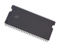
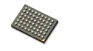
DRAM memory chips are available in a variety of IC package types and with different numbers of pins and flip-flops. Basic IC package types for DRAM memory chips include ball grid array (BGA), quad flat package (QFP), single in-line package (SIP), and dual in-line package (DIP). Many packaging variants are available. For example, BGA variants include plastic-ball grid array (PBGA) and tape-ball grid array (TBGA). QFP variants include low-profile quad flat package (LQFP) and thin quad flat package (TQFP). DIPs are available in either ceramic (CDIP) or plastic (PDIP). Other IC package types include small outline package (SOP), thin small outline package (TSOP), and shrink small outline package (SSOP).
DRAM and SDRAM Memory Chips FAQs
What are the key differences between DRAM and SDRAM in terms of performance and application?
Here are the key differences between DRAM and SDRAM in terms of performance and application.
Performance
Access Time and Speed: DRAM and SDRAM both have access times measured in nanoseconds, which indicates the speed of memory. SDRAM modules are often used in high-speed applications due to their synchronous nature, which allows them to operate in sync with the system clock, improving performance over traditional DRAM.
Data Transfer: SDRAM can handle multiple read/write operations in a single clock cycle due to its ability to access multiple columns once a row is open, which enhances speed and reduces latency.
Applications
DRAM: Used in a variety of applications including desktop and laptop computers, servers, and mobile devices. It is selected based on performance specifications such as access time and refresh rate.
SDRAM: Primarily used in mainstream desktop or server applications. It has replaced older memory technologies like extended data out (EDO) and fast page mode (FPM) modules due to its superior speed and efficiency.
Technology and Design
Synchronous Operation: SDRAM operates synchronously with the system clock, which allows for more efficient data processing compared to asynchronous DRAM.
Bank Interleaving: SDRAM uses bank interleaving to increase performance, allowing each bank to be addressed individually and improving throughput.
What is the role of refresh rate in DRAM performance?
The refresh rate in DRAM plays a crucial role in maintaining data integrity and overall performance. Here are some key points about its role:
Data Integrity
DRAM stores data in capacitors, which tend to lose charge over time. The refresh rate is the frequency at which the stored data is recharged to prevent data loss. This process is essential to maintain the integrity of the data stored in DRAM.
Performance Impact
The refresh rate can affect the performance of DRAM. A higher refresh rate means more frequent recharging of data, which can lead to increased power consumption and potential delays in accessing data. However, it is necessary to ensure data is not lost.
Measurement
The refresh rate is typically expressed in kilobytes (KB) and describes the size of the data that must be recharged.
Self-Refreshing DRAM
Some DRAM chips include self-refreshing technology, which allows them to refresh independently of the CPU or external refresh circuitry. This feature reduces power consumption and is commonly used in devices like notebooks and laptops.
What is the impact of DRAM refresh rate on power consumption?
The impact of the DRAM refresh rate on power consumption is an important consideration in the design and application of DRAM memory chips. Here are some key points:
Power Consumption
The refresh rate directly influences power consumption because it determines how often the DRAM needs to recharge its stored data. A higher refresh rate means the DRAM is refreshed more frequently, which can lead to increased power usage.
Self-Refreshing Technology
Some DRAM chips incorporate self-refreshing technology, which allows them to refresh independently of the CPU or external refresh circuitry. This feature significantly reduces power consumption, making it particularly beneficial for portable devices like notebooks and laptops where power efficiency is crucial.
Balancing Act
What are the advantages of using SDRAM over traditional DRAM?
Here are the advantages of using SDRAM over traditional DRAM:
Synchronous Operation
SDRAM operates in sync with the system clock, which allows for more efficient data processing compared to the asynchronous nature of traditional DRAM. This synchronous operation enhances performance by aligning memory operations with the CPU clock cycles.
Improved Speed and Latency
SDRAM can handle multiple read/write operations in a single clock cycle due to its ability to access multiple columns once a row is open. This capability improves speed and reduces latency, making SDRAM more suitable for high-speed applications.
Bank Interleaving
SDRAM uses bank interleaving to increase performance. This feature allows each bank to be addressed individually, improving throughput and overall memory capacity.
Versatility and Replacement of Older Technologies
SDRAM has replaced older memory technologies like extended data out (EDO) and fast page mode (FPM) modules due to its superior speed and efficiency. It is widely used in mainstream desktop and server applications.
What are the specific applications where SDRAM is most beneficial?
Here are the specific applications where SDRAM is most beneficial:
Mainstream Desktop and Server Applications
SDRAM is widely used in mainstream desktop and server applications due to its superior speed and efficiency compared to older memory technologies like extended data out (EDO) and fast page mode (FPM) modules.
High-Speed Applications
SDRAM's ability to handle multiple read/write operations in a single clock cycle makes it suitable for high-speed applications. Its synchronous operation with the system clock enhances performance by aligning memory operations with CPU clock cycles.
Networking Applications
In networking applications, SDRAM is used to increase bandwidth and ensure signal integrity, which are critical for maintaining efficient data transfer and communication.
Mobile Applications
SDRAM is also beneficial in mobile applications where memory capacity, low power consumption, and compact design are important. Its self-refreshing technology helps reduce power consumption, making it ideal for portable devices like notebooks and laptops.
How does bank interleaving in SDRAM improve performance?
Bank interleaving in SDRAM improves performance through the following mechanisms:
Parallel Access
SDRAM is organized into multiple banks, each of which can be accessed independently. This allows for parallel processing of data, where one bank can be accessed while another is being refreshed or prepared for the next operation. This parallelism reduces wait times and increases throughput.
Reduced Latency
By interleaving banks, SDRAM can reduce latency. When a row in one bank is being accessed, another bank can be precharged and prepared for the next access. This means that the memory controller can switch between banks without waiting for one operation to complete before starting another, effectively hiding the latency associated with row precharge and activation.
Increased Throughput
Bank interleaving allows for successive read/write bursts across different banks, which increases the overall data transfer rate. This is particularly beneficial in applications requiring high-speed data processing, as it maximizes the use of available memory bandwidth.
Efficient Use of Memory Resources
By distributing memory accesses across multiple banks, SDRAM can make more efficient use of its resources, preventing bottlenecks that might occur if all operations were directed to a single bank.
What is the synchronous operation of SDRAM?
The synchronous operation of SDRAM (Synchronous Dynamic Random Access Memory) is a key feature that distinguishes it from traditional DRAM. Here are some important aspects of its synchronous operation:
Synchronization with System Clock
SDRAM operates in sync with the system clock, which means that all operations are timed to coincide with the clock cycles of the CPU. This synchronization allows for more efficient data processing because memory operations can be precisely aligned with the CPU's operations.
Improved Data Processing
By being synchronized with the system clock, SDRAM can handle multiple read/write operations in a single clock cycle. This capability enhances speed and reduces latency, making SDRAM suitable for high-speed applications.
Efficient Memory Access
The synchronous nature of SDRAM allows it to access multiple columns once a row is open, which improves speed and reduces latency through successive read/write bursts. This efficient memory access is a significant advantage over asynchronous DRAM.
Bank Interleaving
SDRAM's architecture includes multiple banks that can be accessed independently. This feature, combined with its synchronous operation, allows for parallel processing of data, reducing wait times and increasing throughput.
DRAM and SDRAM Memory Chips Media Gallery
References
GlobalSpec—White Paper: Design considerations for Teledyne e2v’s space-grade DDR4 (3220083)
GlobalSpec—Dram Modules Information


