FIFO Memory Information
Last revised: October 30, 2024
Reviewed by: Scott Orlosky, consulting engineer
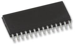
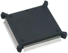
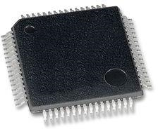
Image Credit: 1-Source Electronic Components
First-in, first-out (FIFO) memory chips are used in buffering applications between devices that operate at different speeds or in applications where data must be stored temporarily for further processing. Typically, this type of buffering is used to increase bandwidth and to prevent data loss during high-speed communications. As the term FIFO implies, data is released from the buffer in the order of its arrival. Some FIFO memory reads with one clock and writes with another simultaneously. Synchronous operations require a clock, but asynchronous operations do not. Flow control generates full and empty signals so that inputs do not overwrite the contents of the buffer. Depending on the device, FIFO memory can be unidirectional or bidirectional. FIFO memory can also include parallel inputs and outputs as well as programmable flags.
Important Specifications
FIFO memory varies in terms of density, number of words, bits per word, supply voltage, and operating temperature. The density is the capacity of the chip in bits. The number of words equals the number of rows, each of which stores a memory word and connects to a word line for addressing purposes. Bits per word are the number of columns, each of which connects to a sense/write circuit. Supply voltages range from - 5 V to 5 V and include intermediate voltages such as -4.5 V, -3.3 V, -3 V, 1.2 V, 1.5 V, 1.8 V, 2.5 V, 3 V, 3.3 V, and 3.6 V. Some FIFO memory chips support a specific temperature range and feature mechanical and electrical specifications that are suitable for commercial or industrial applications. Other FIFO memory chips meet screening levels for military specifications (MIL-SPEC).
How to Select
Selecting FIFO memory requires an analysis of performance specifications such as access time, data rate, data setup time, and data hold time. Measured in nanoseconds (ns), access time indicates the speed of memory and represents a cycle that begins when the CPU sends a request to memory and ends when the CPU receives the data requested. The data rate or transfer speed is the number of bits per second in hertz (Hz) that can be moved internally in the chip. The data setup time is the minimum time interval required for logic levels to be maintained constantly in the input lines prior to the triggering edge of the clock pulse in order for the levels to be reliably clocked into the memory. The data hold time is the minimum time interval required for logic levels to remain on the inputs after the triggering edge of the clock pulse in order to be reliably clocked into the chip.
Technology Families and Packaging
FIFO memory chips vary in terms of logic family and IC package type. Common logic families include standard, fast, high-speed and advanced CMOS; emitter coupled logic (ECL); TTL and Fairchild advanced Schottky TTL (FAST); gunning technology (GTL); and crossbar switch technology (CBT). Common package types include ball grid array (BGA), quad flat package (QFP), single in-line package (SIP), and dual in-line package (DIP). Many packaging variants are available for FIFO chips. Common packaging materials include plastic, ceramic, metal, and glass.
Related Standards
- MIL-M-38510/250 — Microcircuits, Digital, CMOS, 512 X 9 Bit, First In - First Out Dual Port Memory (FIFO), Monolithic Silicon
- SMD 5962-08208 — Microcircuit, Memory, Digital, CMOS, 1k X 36 Clocked FIFO, 3.3 Volt, Radiation-Hardened, Monolithic Silicon
- SMD 5962-97631 — Microcircuit, Memory, CMOS, 32k X 9 Parallel Synchronous FIFO, Monolithic Silicon
FIFO Memory FAQs
What are the differences between SRAM and nvSRAM in the context of FIFO memory?
SRAM (Static RAM) is known for its high speed, making it suitable for applications requiring fast access times. It has low power consumption, which is beneficial for energy-efficient designs. SRAM is volatile, meaning it loses its data when power is turned off.
Due to its speed and low power consumption, SRAM is often used in applications where quick data access is crucial, such as in cache memory and high-speed buffers.
nvSRAM (Non-volatile SRAM) combines the speed of SRAM with non-volatile storage capabilities. Similar to SRAM, nvSRAM also offers low power consumption. Unlike SRAM, nvSRAM retains data even when power is lost, thanks to its non-volatile storage component.
nvSRAM is ideal for applications where data integrity is critical, even in the event of power loss. This makes it suitable for use in systems that require both high-speed access and data retention, such as in industrial control systems and critical data logging.
The primary difference is that nvSRAM retains data without power, whereas SRAM does not. This makes nvSRAM more suitable for applications where data persistence is essential.
SRAM is typically used in scenarios where speed is the primary concern and data loss on power-off is acceptable. In contrast, nvSRAM is used in scenarios where both speed and data retention are required.
How does packaging and integration affect FIFO memory performance?
Packaging factors such as the number of I/O ports, internal frequency, and the presence of integrated phase-locked loops (PLLs) and delay-locked loops (DLLs) can influence the overall performance of FIFO memory.
What are the historical technologies related to FIFO memory?
Legacy technologies include 5 V, 3.3 V, and 2.5 V supply voltages, larger historical fab geometries, and small historical memory sizes. These can impact the performance characteristics of FIFO memory.
What are the different logic families used in FIFO memory?
Transistor-Transistor Logic (TTL) uses transistors as digital switches. It is one of the earliest and most widely used logic families.
Known for its robustness and ease of use, TTL logic is relatively fast but consumes more power compared to some other logic families.
TTL is commonly used in various digital circuits and systems where moderate speed and power consumption are acceptable.
Emitter Coupled Logic (ECL) uses transistors to steer current through gates that compute logical functions.
ECL is known for its high-speed performance, making it suitable for applications requiring very fast data processing.
ECL is often used in high-speed computing and communication systems where speed is a critical factor.
Complementary Metal-Oxide-Semiconductor (CMOS) uses a combination of p-type and n-type metal-oxide-semiconductor field-effect transistors (MOSFETs) to implement logic gates and other digital circuits.
CMOS is known for its low power consumption and high noise immunity, making it ideal for battery-operated devices and systems requiring energy efficiency.
CMOS is widely used in a variety of applications, including microprocessors, microcontrollers, and other integrated circuits.
Cross-Bar Switch Technology (CBT) is a type of logic family used for digital comparators and other specialized applications.
CBT is known for its ability to handle multiple data paths simultaneously, enhancing data throughput. It is used in systems requiring high data transfer rates and efficient data routing.
Gallium Arsenide (GaAs) is a compound semiconductor used in high-speed and high-frequency applications. It offers superior electron mobility compared to silicon, resulting in faster switching speeds and higher frequency operation.
GaAs is commonly used in microwave and millimeter-wave devices, as well as high-speed digital circuits.
Integrated Injection Logic (I2L) is a type of bipolar logic family known for its low power consumption. It combines the advantages of bipolar and MOS technologies, offering moderate speed and low power usage.
I2L is suitable for applications where power efficiency is a highly desired feature, such as portable and battery-operated devices.
Silicon on Sapphire (SOS) technology involves the use of a thin layer of silicon on a sapphire substrate. It provides high radiation resistance and low parasitic capacitance, making it suitable for harsh environments.
SOS is used in aerospace, military, and other applications requiring high reliability and radiation hardness.
Gunning Transceiver Logic (GTL) and Gunning Transceiver Logic Plus (GTLP) are logic families designed for high-speed data transmission. They are known for their low voltage swing and high-speed performance, reducing power consumption and electromagnetic interference. They are commonly used in high-speed data buses and communication interfaces.
What are the applications of SRAM in FIFO memory?
SRAM is known for its high speed, making it ideal for use in high-speed buffer applications.
In systems where data needs to be temporarily stored and quickly accessed, such as in networking equipment and communication systems, SRAM-based FIFO memory can provide the necessary speed and efficiency.
SRAM's fast access times make it suitable for use as cache memory.
In processors and computing systems, SRAM-based FIFO memory can be used to store frequently accessed data, reducing the time it takes to retrieve this data and improving overall system performance.
SRAM's low power consumption and high speed are beneficial for data logging applications.
In industrial control systems and scientific instruments, SRAM-based FIFO memory can be used to log data at high speeds, ensuring that critical information is captured accurately and efficiently.
The high-speed nature of SRAM makes it suitable for real-time data processing applications.
In applications such as video processing, audio processing, and real-time analytics, SRAM-based FIFO memory can handle the rapid data throughput required for real-time operations.
SRAM's low power consumption and fast access times are advantageous for embedded systems.
In embedded systems used in automotive, medical devices, and consumer electronics, SRAM-based FIFO memory can provide the necessary performance while maintaining energy efficiency.