Field-Programmable Gate Arrays (FPGA) Information
Last revised: October 31, 2024
Reviewed by: Scott Orlosky, consulting engineer
 Field-programmable gate arrays (FPGAs) are integrated circuits (ICs) that contain an array of logic cells surrounded by programmable I/O blocks. FPGAs contain as many as hundreds of thousands, up to millions of logic cells and an even greater number of flip-flops. Because of cost, field-programmable gate arrays do not provide a 100% interconnection between logic cells; however, FPGAs still provide significantly higher capacities than programmable logic devices (PLDs) that are interconnected through a central global routing pool.
Design engineers use field-programmable gate arrays to program electrical connections through several iterations in order to minimize non-recurring costs. FPGAs are used in applications ranging from data processing and storage, to instrumentation, telecommunications, and digital signal processing. Other terms for FPGA include logic cell array (LCAs) and programmable application-specific integrated chip (pASIC).
Component Types
Field-programmable gate arrays are available with different numbers of system gates, shift registers, logic cells, and look up tables. Logic blocks or logic cells (LCs) do not include I/O blocks, but generally contain a look up table to generate any function of inputs, a clocked latch (flip-flop) to provide registered outputs, and control logic circuits for configuration purposes. Logic cells are also known as logic array blocks (LABs), logic elements (LEs) and configurable logic blocks (CLBs). Look-up tables (LUTs) or truth tables are used to implement a single logic function by storing the correct output logic state in a memory location that corresponds to each particular combination of input variables.
Requirement Selections
Selecting field-programmable gate arrays requires an analysis of memory, performance, and I/O interface requirements. Available memory types include:
- Content addressable memory (CAM)
- Flash, random access memory (RAM)
- Dual-port RAM
- Read-only memory (ROM)
- Electrically erasable programmable read-only memory (EEPROM)
- First-in, first-out (FIFO)
- Last-in, first out (LIFO)
Performance considerations include internal frequency, the number of integrated phase-locked loops (PLLs) and delay-locked loops (DLLs) with clock-frequency-synthesis capabilities, and the total number of I/O ports. I/O interfaces for field-programmable gate arrays include accelerated graphics port (AGP), bus low voltage differential signaling (BLVDS), and peripheral component interconnect (PCI).
Field-Programmable Gate Arrays Options
 Field-programmable gate arrays are available with many logic families. Transistor-transistor logic (TTL) and related technologies such as Fairchild advanced Schottky TTL (FAST) use transistors as digital switches. By contrast, emitter coupled logic (ECL) uses transistors to steer current through gates that compute logical functions. Another logic family, complementary metal-oxide semiconductor (CMOS), uses a combination of P-type and N-type metal-oxide-semiconductor field effect transistors (MOSFETs) to implement logic gates and other digital circuits. Logic families for field-programmable gate arrays include:
- Crossbar switch technology (CBT)
- Gallium arsenide (GaAs)
- Integrated injection logic (I2L)
- Silicon on sapphire (SOS)
- Gunning with transceiver logic (GTL) and
- Gunning with transceiver logic plus (GTLP) for field-programmable gate arrays are also available.
Packaging Options
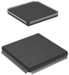
Field-programmable gate arrays are available in a variety of IC package types and with different numbers of pins and flip-flops. Basic IC package types for field-programmable gate arrays include:
- Ball grid array (BGA)
- Quad flat package (QFP)
- Single in-line package (SIP)
- Dual in-line package (DIP)
Many packaging variants are available. For example, BGA variants include plastic-ball grid array (PBGA) and tape-ball grid array (TBGA). QFP variants include low-profile quad flat package (LQFP) and thin quad flat package (TQFP). DIPs are available in either ceramic (CDIP) or plastic (PDIP). Other IC package types for field-programmable gate arrays include small outline package (SOP), thin small outline package (TSOP), and shrink small outline package (SSOP).
Standards
- JEDEC JESD 12 — Standard for Gate Array Benchmark Set
- JEDEC JESD 12-3 — CMOS Gate Array Macrocell Standard
Field-Programmable Gate Arrays (FPGA) FAQs
How do FPGAs differ from ASICs?
FPGAs are integrated circuits that can be programmed and reprogrammed to perform specific tasks, unlike ASICs which are custom-designed for a particular application. FPGAs offer design flexibility, faster time-to-market, and lower non-recurring engineering costs, making them suitable for prototyping and applications requiring frequent updates or bug fixes.
What are the main components of an FPGA?
An FPGA typically consists of configurable logic blocks (CLBs), configurable I/O blocks, and programmable interconnects to route signals between these blocks. Additional resources such as ALU (Arithmetic Logic Units), memory, and decoders may also be available.
What are the advantages of using FPGAs?
FPGAs provide design flexibility, faster time-to-market, lower technical risk, and the ability to reprogram in the field. They are beneficial for applications that may require frequent updates or bug fixes and offer obsolescence mitigation by allowing firmware code to be ported to next-generation devices
What are some common applications of FPGAs?
FPGAs are used in various application groups including consumer electronics, medical, industrial, automotive, and wireless communication. They are particularly useful in applications requiring high volume, low power, quick time-to-market, embedded computing, signal processing, and high-speed signal interfaces.
How do FPGAs compare to microprocessors or microcontrollers?
Unlike microprocessors or microcontrollers, which execute specific instructions and have a fixed set of interfaces, FPGAs are not limited to predefined logic blocks and can be configured to perform a wide range of tasks.
What are the differences between static RAM (SRAM) and antifuse technologies in FPGAs?
Configuration and Volatility
SRAM-based FPGAs: These use static RAM to store the logic configuration. SRAM is volatile, meaning it loses its data when power is removed. Therefore, SRAM-based FPGAs need to be reprogrammed each time the system is powered on. They support in-system programming (ISP), allowing them to be configured or reconfigured without being removed from the board.
Antifuse-based FPGAs: Antifuse technology is non-volatile, meaning the configuration is retained even when power is removed. These are one-time programmable (OTP) devices, meaning once they are programmed, they cannot be reprogrammed. This makes them suitable for applications where the configuration does not need to change.
Programming Flexibility
SRAM-based FPGAs: Offer flexibility in programming and reprogramming, which is beneficial for prototyping and applications requiring frequent updates or bug fixes.
Antifuse-based FPGAs: Once programmed, the configuration is permanent, which can be advantageous for security and reliability in certain applications where reprogramming is not needed.
Power Consumption
SRAM-based FPGAs: Typically require more power because they need to maintain the configuration in volatile memory.
Antifuse-based FPGAs: Generally consume less power since they do not need to maintain a volatile configuration.
How do SRAM-based FPGAs support in-system programming?
There are several mechanisms that allow them to be configured or reconfigured without being removed from the board. Here are the key aspects of how they achieve this:
SRAM-based FPGAs can be configured using different methods such as synchronous serial, parallel, and JTAG interfaces. These methods allow the FPGA to be programmed while it is still on the board, which is a key feature of in-system programming.
The most common sources for configuring SRAM-based FPGAs include:
In-system discrete configuration memory, such as a programmable read-only memory (PROM) or Flash memory device.
On-board or in-system processor with access to nonvolatile memory.
JTAG connection attached to a PC, which is often used for development and debugging purposes.
Programming Modes
SRAM-based FPGAs can operate in master mode, where they read configuration data from an external source like a Flash memory chip, or in slave mode, where they are configured by an external master device such as a processor. This flexibility supports ISP by allowing the FPGA to be programmed directly on the board.