Properties of Porous Silicon

1.2: Porous Silicon Formation by Anodisation

1.2 Porous Silicon Formation by Anodisation

A. Halimaoui
August 1997

A POROUS SILICON FORMATION: ANODISATION CELLS

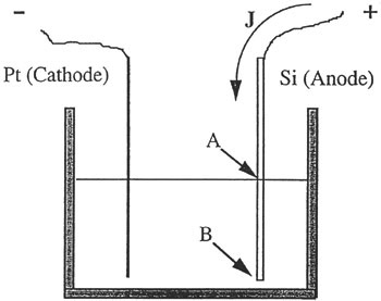
Porous silicon (PS) is known to form during electrochemical dissolution of silicon in HF-based solutions. This dissolution is obtained by monitoring either the anodic current or potential. In general, constant current is preferable, as it allows a better control of both the porosity and thickness and a good reproducibility from run to run. The simplest cell which can be used to anodise silicon is shown in FIGURE 1. The silicon wafer serves as the anode. The cathode is made of platinum or any HF-resistant and conducting material. The cell body itself is, in general, made of highly acid-resistant polymer such as Teflon. Since the entire silicon wafer serves as the anode, PS is formed on any wafer surface in contact with the HF solution, including the cleaved edges. The advantage of such equipment is its simplicity and ability to anodise silicon-on-insulator structures. Its drawback is the non-uniformity in both the porosity and thickness of the resulting layer. This inhomogeneity is mainly due to a lateral potential drop. In fact, since the current flows laterally along the bulk of the silicon wafer, there is a difference in potential between the top (point A in FIGURE 1) and the bottom (point B in FIGURE 1). The potential drop across the wafer leads to different values of the local current density which induce porosity and thickness gradients.


Figure 1: Cross-sectional view of a 'lateral anodisation cell'.

The...

UNLIMITED FREE
ACCESS
TO THE WORLD'S BEST IDEAS

SUBMIT
Already a GlobalSpec user? Log in.

This is embarrasing...

An error occurred while processing the form. Please try again in a few minutes.

Customize Your GlobalSpec Experience

Category: Wafer and Thin Film Instrumentation
Finish!
Privacy Policy

This is embarrasing...

An error occurred while processing the form. Please try again in a few minutes.