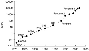
TCAD for Si, SiGE and GaAs Integrated Circuits

In the field of microelectronics, the planar Si metal-oxide-semiconductor field-effect transistor (MOSFET) is perhaps the most important invention. It started in 1928 when J.E. Lilienfeld proposed the concept of field-effect conductivity modulation and the MOSFET [1]. With the discovery of silicon dioxide (SiO 2) passivation for the Si semiconductor system by Atalla in 1958, the modern Si MOSFET era started [2]. Since then MOSFET performance has improved at a dramatic rate owing to gate length scaling and has become the dominant technology for integrated circuits.
During the early years of transistor scaling, Gordon Moore predicted that the number of transistors in a chip will increase exponentially [3, 4], which is now known as Moore's law. However, according to Moore himself, 'no exponential is forever' [5]. Many of the exponential trends are approaching limits that require new means to circumvent to continue the historic rate of progress. Accordingly, new and more fundamental barriers must be confronted in the coming decades - the fact that the technology is approaching atomic dimensions. For example, Figure 4.1 shows the increase in computer performance benefiting from both faster transistors and an exponentially increasing transistor budget. Figure 4.2 shows the increasing power dissipation of microprocessor chips, despite all attempts to decrease operating voltage (see Figure 4.3) and minimise leakage currents.