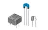
5.6.1 Electrical Properties
The potential applications of plasma polymers in electronics, as it follows from the previous parts of the chapter, are wide and very promising. The main advantage of these materials is that they can be deposited easily in the form of thin films, at low temperature and low costs, on inexpensive substrates of almost any size or shape. In some cases the plasma polymer films have been already brought into practice, in others considerable effort is focused on finding their technological application.
In the beginning when plasma polymers emerged, i.e. in the sixties, a great deal of attention was paid first of all to dielectric and insulating properties of the films. The attempts to apply these materials in the electronics field, as thin-film capacitors as well as insulating and corrosion-protecting coatings of electronic devices, were undertaken. The works of Goodman [196], Bradley and Hammes [197], [198], Stuart [199], [200], Ozawa [201], Bashara and Doty [202], Gregor [203], Mearns [204], and Babcock and Christy [205] constituted the most significant basis to develop this new class of amorphous insulators.
At the same time, in 1965, the first semiconducting films (a-Si:H and a-Ge:H) were fabricated as well [105]. However, they were not "discovered" for electronics before the mid-1970s, when the doping effect was found out [107]- [109]. A huge progress in the technological application of semiconducting plasma polymers has been achieved ever since.


 TABLE OF CONTENTS