Electronic Materials and Processes Handbook, Third Edition

Dr. Jerry E. Sergent
School of Engineering
Fairfield University
Fairfield, Connecticut
Hybrid microelectronics technology is a distinct branch of electronics packaging technology and is primarily differentiated from other branches by the manner in which the interconnection patterns are generated. The foundation for the hybrid circuit is a substrate fabricated from one of the refractory ceramics. A metallization pattern is created on the substrate by one of the film technologies, forming the mounting pads and circuit traces to which we bond and interconnect additional active and passive devices as necessary. Another characteristic of hybrid technology is the ability to fabricate passive components. The thick and thin film technologies, for example, can be used to manufacture resistors with parameters superior to those of carbon resistors that are commonly used in conjunction with printed circuit boards.
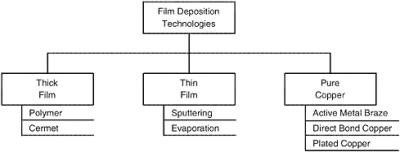
The most commonly accepted definition of a hybrid circuit is a ceramic substrate metallized by one of the methods shown in Fig. 8.1, containing at least two components, one of which must be active. This definition is intended to exclude single-chip packages and circuits that contain only passive components such as resistor networks. By this definition, a hybrid circuit may range from a simple diode-resistor logic gate to a circuit containing in excess of 100 integrated circuits (ICs).
Multichip modules (MCMs) are close relatives of hybrid circuits. Although many of the assembly processes are common to those used to fabricate hybrid circuits, MCMs, as shown in Fig. 8.2, employ...