Introduction to Modeling HBTs
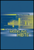
A basic knowledge of semiconductor device physics is necessary if one attempts to understand a bipolar transistor model or develop a new version of a model. However, it is not the aim of this chapter to give a comprehensive introduction. Rather some results are recalled, in order to provide a link from the phenomena observed in HBT operation to the physical background. For an in-depth explanation or a detailed introduction into bipolar transistor physics, please refer to the literature (e.g., [1 5]).
Three topics are addressed here:
The forward-biased pn junction, in order to explain the emitter-base junction and the injection of electrons into the base;
The transport of minority carriers through neutral bulk material, as in the base;
The reverse biased pn junction in the presence of an electron current, as it occurs in the base-collector junction, when collector current is flowing.
The examples will be given for npn transistors, since this is the common configuration for HBTs.
First, some properties of an abrupt pn junction will be reviewed.
We will focus on the low-injection condition first, which means that the number of minority carriers is very small in the n and p regions. In this case, the majority carrier density in the neutral regions is approximately not affected by diffusion currents of minority carriers. At the junction, the doping abruptly changes from n type to p type. This implies a steep gradient in doping concentration resulting in diffusion of...