Optics of Quantum Dots and Wires
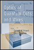
Quantum technology is the key to next-generation optoelectronics and laser semiconductors, and this cutting-edge book is an in-depth examination of how quantum dots and wires are fabricated and applied to optics.
 TABLE OF CONTENTS
 Low-dimensional QWR and QD optoelectronic devices have been predicted to exhibit improved performance and new functionality as compared with more conventional QW devices [6, 7, 17]. The potential improvement of QWR and QD optical modulators, switches, detectors, and lasers relies on the enhanced optical absorption, refraction, and optical gain related to the peaked density of states, and the enhancement of excitonic and other Coulomb correlation effects due to the multidimensional quantum confinement. However, to fulfill these expectations, the corresponding QWR and QD heterostructures should exhibit high interface quality to avoid nonradiative carrier recombination, and high uniformity to minimize inhomogeneous broadening effects. Moreover, to be compatible with optoelectronic devices, the wires and dots should be incorporated in tight optical waveguides or cavities, or else should be produced with high surface densities, to optimize the interaction with the electromagnetic field. Efficient routes for carrier transport from the device contacts into the 1D or 0D potential wells are also highly desirable for minimizing leakage currents.
The high interface quality, the uniformity, and the unique configurations achievable with V-groove QWs and QWRs are useful for a number of novel optoelectronic devices, which are described in this section in some detail. It should be noted that the density of wires and dots that can be obtained with this technique is limited by the lithographic technique used to define the substrate patterns. So far, the fabrication of 250-nm pitch V-groove QWRs has been demonstrated using holographic lithography. By e-beam lithography it...