Printed Circuit Assembly Design

Chapter 3: Design Process Flow

Overview

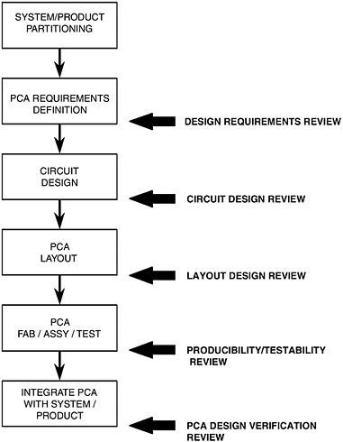
The process flow diagram in Fig. 3.1 shows the normal sequence of activities in the printed circuit assembly (PCA) design process and their relationship to each other. It displays the general chronology of the design effort, but it does not show the iteration and feedback paths inherent in a typical design effort.


Figure 3.1: PCA design reviews.

Ideally, each step in the PCA design process should be accomplished in a logical sequence, and there should be as few loop-backs, or repeated activities, as possible. Since this is not a perfect world, such an ideal is rarely achieved. Therefore, in order to maximize the cost and schedule efficiency of a PCA design effort, review checkpoints, or gateways, should be established at critical points in the process. Successful completion of a review can minimize the risk that some part of the design activities preceding the review was done improperly. The process flow diagram in Fig. 3.1 indicates the points in the process where design reviews are most effective.

It is important that organizational functions that are directly or indirectly involved in the life cycle of a PCA should be participants in these reviews. Any or all of the following could be included:

  • The project engineer responsible for the overall PCA design

  • The PCA circuit design engineer

  • The board layout designer

  • The engineer responsible for integrating the PCA into the next level of assembly

  • Production engineering

  • Test engineering

  • Components engineering

  • Engineers responsible for...

UNLIMITED FREE
ACCESS
TO THE WORLD'S BEST IDEAS

SUBMIT
Already a GlobalSpec user? Log in.

This is embarrasing...

An error occurred while processing the form. Please try again in a few minutes.

Customize Your GlobalSpec Experience

Category: Computer-Aided Design (CAD) Services
Finish!
Privacy Policy

This is embarrasing...

An error occurred while processing the form. Please try again in a few minutes.