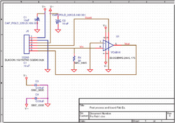
Complete PCB Design Using OrCad Capture and Layout

Chapter 10: Postprocessing and Board Fabrication

Postprocessing was briefly introduced in Chap. 2. In Chap. 10 we look at postprocessing in greater detail and show how to submit the Gerber files to an actual board house (Advanced Circuits).

The Circuit Design with OrCAD

Schematic design in Capture

As with the previous examples, we will use a simple circuit to minimize details and allow us to focus on the board layout. The circuit (shown in Fig. 10-1) consists of a six-pin PCB connector (J1), bulk decoupling capacitors (C1 and C2), a variable gain amplifier (U1), bypass capacitors (C3 and C4), and a terminating resistor (R1). Once we move the design to Layout we will add different types of mounting holes so that when we postprocess the design you will be able to see the different types of drill files that are generated. The circuit contains only 7 parts so that if you are using the Demo version the total part count is only 10 (including the mounting holes), so that the design can be saved and postprocessed.


Figure 10-1: The circuit design for fabrication.

The footprints for each of the components are shown on the schematic. To display component information on the schematic double click the part to display the Property Editor spreadsheet (see Fig. 10-2). Select the cell (row or column) that contains the information you want displayed. Click the Display button at the top of the spreadsheet to show the Display Properties dialog box. Select one of the display...

UNLIMITED FREE
ACCESS
TO THE WORLD'S BEST IDEAS

SUBMIT
Already a GlobalSpec user? Log in.

This is embarrasing...

An error occurred while processing the form. Please try again in a few minutes.

Customize Your GlobalSpec Experience

Category: PCB Design and Layout Services
Finish!
Privacy Policy

This is embarrasing...

An error occurred while processing the form. Please try again in a few minutes.