Fabrication of GaAs Devices

The purpose of this section is to give an introduction to methods of qualifying substrates, epitaxial samples for device fabrication, and often in-process or finished devices. One goal is to identify bad samples to discard them before the high cost of doing epitaxial growth and processing them into devices is incurred. Another goal is to identify problems with epitaxial growths as soon as possible so that they can be corrected before large amounts of material must be scrapped. Lastly, many of these techniques are used in failure analysis for devices that either did not meet specifications or have failed in operation before their expected lifetime. The process engineer should have a rudimentary knowledge of these techniques so that interactions between different groups of engineers for the purpose of quality improvement or failure analysis can be fruitful in determining the often complex interactions between materials, processing and assembly. For greater detail than is available in this section, refer to references [11,12].
Optical techniques presented in this section include optical microscopy, ellipsometry, photoluminescence, X-ray photoelectron spectroscopy (XPS) and X-ray diffraction.
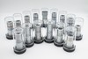
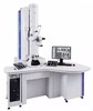
The most obvious and widely useful characterisation technique is optical microscopy. Optical microscopes take collimated light that is reflected (usually) off a sample and imaged through a high-quality lens system to eyepieces or to a video camera. Objectives with different magnification can be switched in and out to allow the user a range typically between 50- and 500-fold magnification. Microscopes are marvellous instruments that make complex...