5.2 Silicon Nanowire MOSFETs
The approach of Chapter 3 can be used to establish some general features of semiconductor nanowire MOSFETs. We assume a very simple geometry as shown in Fig. 5.1 - a nanowire that is coaxially gated. Instead of C ins = K ins ? 0/ t ins F/cm 2 as for a MOSFET, we have an insulator capacitance of
| (5.1) | 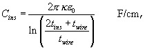
|
where t wire is the diameter of the wire.
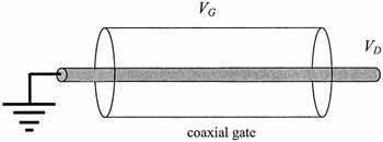 Figure 5.1: The geometry of a simple, idealized coaxial gate nanowire MOSFET.
 We first need to evaluate some directed moments analogous to Eqns. (3.5). Specifically, we must evaluate
| (5.2a) | 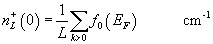
|
| (5.2b) | 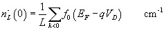
|
| (5.2c) | 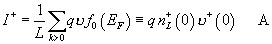
|
| (5.2d) | 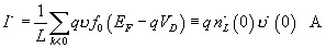
|
We will work within the effective mass approximation and assume a simple, parabolic bandstructure,
| (5.3) | 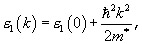
|
where ? 1(0) is the minimum of the first subband at the top of the barrier. We assume that only one subband is occupied, so the directed moments can be evaluated to find
| (5.4a) | 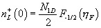
|
| (5.4b) | 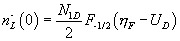
|
| (5.4c) | 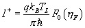
|
| (5.4d) | 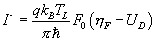
|
| (5.4e) | 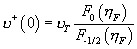
|
| (5.4f) | 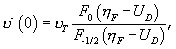
|
where ? F = ( E F- ?(0))/ k BT L, U D = qV D/ k BT L, and 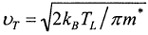 as before. The one-dimensional effective density of states is
| (5.4g) | 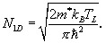
|
It is important to note that the expressions for the directed currents are independent of the bandstructure, because when converting the sum over k-states to an integral over energy, the density of states cancels with the velocity in Eqns. (5.2c) and (5.2d).
5.2.1 Evaluation of the...