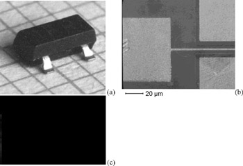
Nanotechnology and Nanoelectronics: Materials, Devices, Measurement Techniques

At present, development in electronic devices means a race for a constant decrease in the order of dimension. The general public is well aware of the fact that we live in the age of microelectronics, an expression which is derived from the size (1 ?m) of a device's active zone, e.g., the channel length of a field effect transistor or the thickness of a gate dielectric. However, there are convincing indications that we are entering another era, namely the age of nanotechnology. The expression "nanotechnology" is again derived from the typical geometrical dimension of an electronic device, which is the nanometer and which is one billionth (10 ?9) of a meter. 30,000 nm are approximately equal to the thickness of a human hair. It is worthwhile comparing this figure with those of early electrical machines, such as a motor or a telephone with their typical dimensions of 10 cm. An example of this development is given in Fig. 1.1.
From the industrial point of view, it is of great interest to know which geometrical dimension can be expected in a given year, but the answer does not only concern manufacturers of process equipment. In reality, these dimensions affect almost all electrical parameters like amplification, transconductance, frequency limits, power consumption, leakage currents, etc. In...