In chapters 2 and 3 several possible implementations for integrated current conveyors have been presented. In particular, we have focused our attention on the LV LP solutions.
If there is not a particular need of LV LP topologies (or it is not possible to design and fabricate a chip dedicated to a CCII-based application), a component commercially available can be the best solution. Such a component is the Analog Device AD844, whose simplified block scheme is shown in figure C.1.
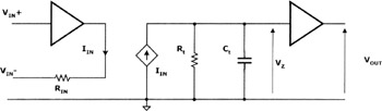 Figure C.1: AD844 block scheme
 The input stage is represented by a voltage buffer and a R IN resistance. The node V IN+ shows a high impedance, while V IN ? shows a low one, ideally zero. When a voltage is applied to V IN+ and a load is connected to V IN ?, a current named I IN flows in this load. This current can be found also at the output stage, represented as the current source I IN. The load connected to this current source represents the transresistance of the AD844 amplifier. The ratio between R t and R IN is the voltage gain, having a typical value of 60000, while current gain is about 40000.
At the output we have two nodes: a high impedance node (Z) and a low impedance one (OUT). According to the theory presented in the first chapter, this device can be considered as a Current Feedback Operational Amplifier (CFOA). It is interesting to...
Copyright Kluwer Academic Publishers 2003 under license agreement with Books24x7


 TABLE OF CONTENTS