Multigroup Equations for the Description of the Particle Transport in Semiconductors

Chapter 10: Simulation of Gallium Arsenide Devices

10.1 Introduction

In this chapter, we present numerical results for the transport of electrons in bulk GaAs, in a GaAs n + - n i - n + diode and in a GaAs-MESFET obtained by means of our multigroup approach (8.17). All of these calculations are performed for the lattice temperature T L = 300 K. We approximate the conduction band of GaAs by taking into account the ?-valley in the center of the first Brillouin zone and four equivalent L-valleys along the crystallographic directions ?1, 1, 1 ?. The zero energy level is set to the energy of the bottom of the ?-valley, in other words, ? 0? = 0. In our transport model for GaAs, we regard the acoustic deformation potential scattering (ADP) with the transition rate

(10.1)

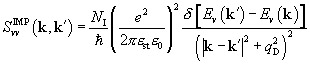
and the ionized impurity scattering (IMP)

(10.2)

with the screening parameter = e 2 N I/ ? st ? 0 k B T L. The most important intravalley scattering mechanism for GaAs is the polar optical interaction (POP) with the transition rate

(10.3)
Table 10.1: Material parameters for GaAs.

Quantity

Symbol

Unit

Value

Mass density

?

kgm -3

5360

Sound velocity

v s

ms -1

5240

Static dielectric constant

? st

12.90

High-frequency dielectric constant

? hf

10.92

Acoustic deformation potential

D A

eV

7

Optical deformation potential

D O

eVm -1

10 11

Non-polar optical phonon energy

UNLIMITED FREE
ACCESS
TO THE WORLD'S BEST IDEAS

SUBMIT
Already a GlobalSpec user? Log in.

This is embarrasing...

An error occurred while processing the form. Please try again in a few minutes.

Customize Your GlobalSpec Experience

Category: Optical Crystals
Finish!
Privacy Policy

This is embarrasing...

An error occurred while processing the form. Please try again in a few minutes.